Production method for through wafer interconnection construction

An interconnection structure and through-silicon via technology, applied in semiconductor/solid-state device manufacturing, electrical components, circuits, etc., can solve problems such as increased cost, long working hours, and excess, to alleviate thermal mismatch, reduce parasitic capacitance, reduce Effects of thermomechanical stress

Active Publication Date: 2009-07-15
HUAZHONG UNIV OF SCI & TECH
View PDF0 Cites 43 Cited by
  • Summary
  • Abstract
  • Description
  • Claims
  • Application Information

AI Technical Summary

Problems solved by technology

[0005] This process flow can effectively realize high-density three-dimensional through-hole interconnection, but there are the following problems: (1) there is only a very thin insulating layer (usually silicon dioxide) between the silicon substrate and the copper structure layer , which leads to the formation of high capacitance between TSV interconnects, sometimes even exceeding the capacitance of standard wire-bonded interconnects; (2) fairly thick copper structures are filled in silicon holes
Due to the large thermal mismatch between silicon and copper, this will cause significant thermomechanical stress during thermal cycling; (3) the method of fully filling silicon holes with electroplated copper requires a long man-hour, which increases the process method cost

Method used


Image

  • Production method for through wafer interconnection construction
  • Production method for through wafer interconnection construction

Examples


Embodiment Construction

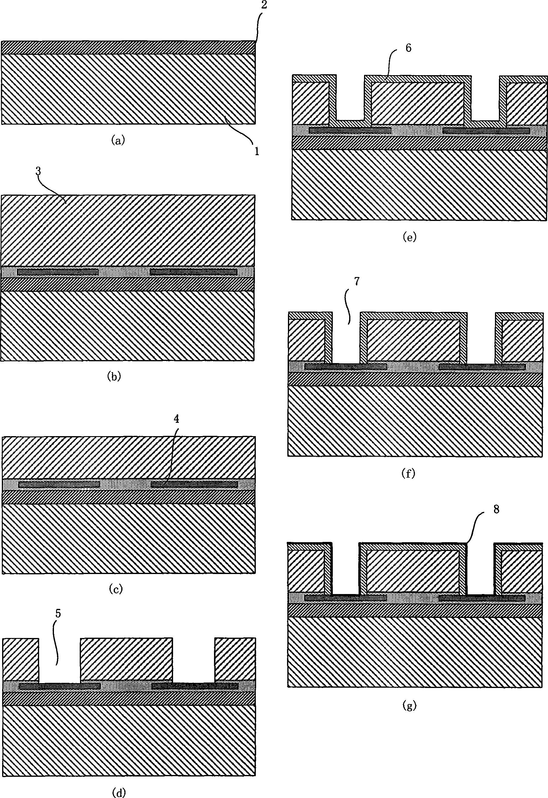
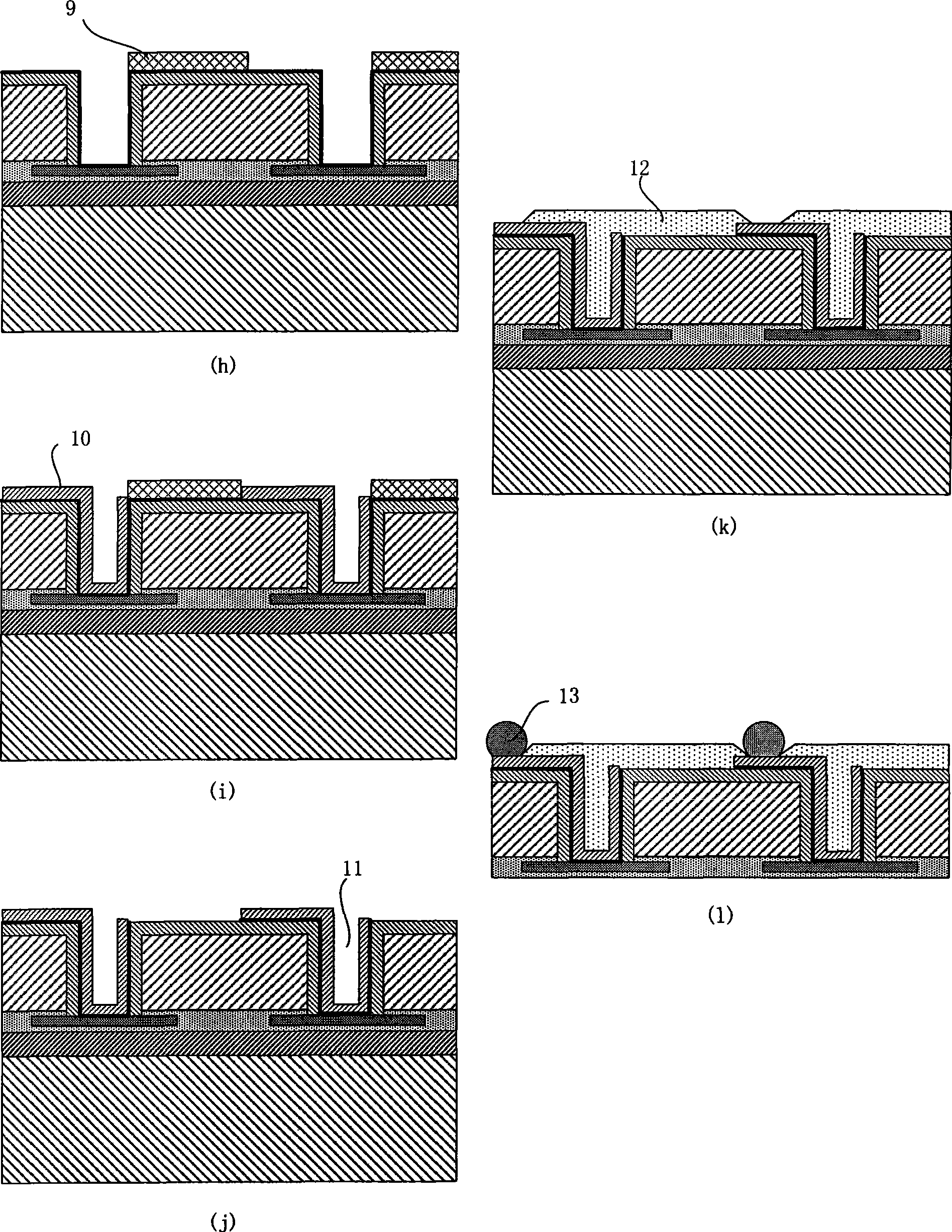
[0019] The specific embodiments of the process method provided by the present invention will be described in further detail below with reference to the accompanying drawings and examples. The method of the present invention includes:

[0020] (a) Provide a substrate 1 , such as a silicon wafer coated with an oxide layer 2 . The thickness of the substrate is 10-500 microns. see figure 1 (a).

[0021] (b) Bonding a silicon device wafer or chip 3 having at least one internal contact 4 on the silicon wafer. For example, aluminum pads and passivation layers can be fabricated on the front side of the device wafer or chip by flip-chip method to form internal contact points 4 . see figure 1 (b).

[0022] (c) Thinning silicon device wafers or chips by mechanical grinding. The grinding thickness is 25-100 microns. see figure 1 (c).

[0023] (d) dry etching the silicon device wafer or chip to form blind vias 5, the blind vias 5 having an aspect ratio of 5:1-20:1. These blind h...


PUM

PropertyMeasurementUnit
thicknessaaaaaaaaaa
thicknessaaaaaaaaaa

Abstract

The invention discloses a through wafer interconnect structure preparation method comprising: 1. bonding a bonding silicon device wafer on a silicon wafer substrate; 2. thinning the silicon device wafer, etching the silicon device and forming a blind hole; 3. coating a layer of pattern dielectric material (such as poly-p-xylene) on the silicon device wafer; 4. etching the pattern dielectric substance layer, etching the dielectric material at the bottom of the blind hole, keeping a blind hole side wall; forming a dielectric substance hole on the substrate and enabling the dielectric substance hole and the blind hole coaxial; 5. depositing a layer of conductive material on the dielectric substance hole as a conductive layer and forming a conductive hole; 6. re-depositing a layer of pattern dielectric substance on the conductive layer; 7. forming a solder micro-convex point on the conductive layer. The invention simplifies the process steps, reduces the process time and the cost; depresses a parasitic capacitance, improves a interconnect electrical behavior, suits for the RF three-dimensional interconnection structure; releases the thermal mismatch between the conductive material and the silicon and greatly reduces the thermal mechanical stress.

Description

technical field [0001] The invention belongs to an electrical interconnection processing technology in the field of extremely large-scale integrated circuit manufacturing, and is particularly suitable for processing system-in-package (SiP), system-on-chip (SoC) and three-dimensional stacked through-silicon-via (TSV) interconnect structures. technical background [0002] For the past four decades, the research, development, and production of microelectronic components has continued in the direction predicted by Moore's Law. In 2008, several companies, including Intel, started using 45- to 50-nanometer processing technology in the mass production of memory chips. According to this development trend, by 2012 at the latest, in order to further improve the integration of the chip, it is necessary to use 32 or even 22 nanometer processing technology. However, the processing technology of 32 or 22 nanometers not only encounters the limitations of lithography equipment and technolo...

Claims


Application Information

Patent Timeline
Patent Type & Authority Applications(China)
IPC IPC(8): H01L21/768
CPCH01L21/76898
Inventor 刘胜高鸣源胡程志吴一明
Owner HUAZHONG UNIV OF SCI & TECH
Why Eureka
Try Eureka