Method for cutting graphite alkene by titanium dioxide photocatalysis

A technology of titanium dioxide and graphene, which is applied in the field of tailoring and modification of nanomaterial structures, can solve problems such as low efficiency and incompatibility of semiconductor processes

Inactive Publication Date: 2009-08-12
PEKING UNIV
View PDF0 Cites 28 Cited by
  • Summary
  • Abstract
  • Description
  • Claims
  • Application Information

AI Technical Summary

Problems solved by technology

This method is inefficient and is not compatible with current semico

Method used


Image

  • Method for cutting graphite alkene by titanium dioxide photocatalysis
  • Method for cutting graphite alkene by titanium dioxide photocatalysis
  • Method for cutting graphite alkene by titanium dioxide photocatalysis

Examples


Embodiment 1

[0035] Cut graphene as follows:

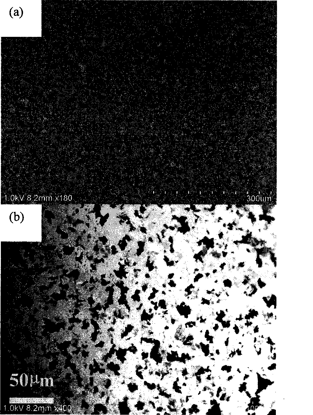
[0036] 1) On Si / SiO 2 Substrate (Si layer thickness is 600 microns, SiO 2 The substrate layer is 300 nanometers), and electron beam vapor deposition of 500 nanometers of metal nickel is carried out after annealing, and chemical vapor deposition growth is carried out, so that graphene sheets are precipitated on the nickel surface. Transferring graphene to another sheet of Si / SiO 2 On the substrate, the average thickness of the graphene sheet is within 10 nanometers. Among them, the annealing temperature is 900-1000°C, the atmosphere is argon 600sccm / hydrogen 500sccm, and the time is 10-20 minutes; the growth temperature is 900-1000°C, the growth time is 5-10 minutes, and the carbon source is methane. The transfer step uses polymethyl methacrylate (PMMA) as the medium. SEM image of transferred graphene as figure 2 shown; among them, figure 2 (a) is a low-resolution SEM image, figure 2 (b) is a high-resolution SEM image.

[0037] 2) Us...

Embodiment 2

[0041] 1) Prepare a mixed solution of 0.5 mg / ml graphite oxide in methanol / water (volume ratio 2:1), pipette 25 microliters dropwise onto Si / SiO 2 Substrate (Si layer thickness is 600 microns, SiO 2 The substrate layer is 300 nanometers) surface, and dried at 70° C. for 1 hour to obtain a graphite oxide film, which is then thermally reduced to obtain a graphene sheet. Wherein the thermal reduction time is controlled at 1 hour, and the flows of argon and hydrogen are both 300 sccm. The scanning electron microscope image of the resulting graphene is as Figure 5 shown.

[0042] 2) Spin-coat photoresist on the quartz substrate, and sequentially adopt photolithographic exposure, development, and fixation to build a titanium dioxide micro-nano structure on the surface of the quartz substrate; Dissolves the photoresist on the quartz surface.

[0043] Among them, the photoresist is positive resist AR-P5350, the spin coating speed is 4000 rpm, and the time is 1 minute; then the qu...

Embodiment 3

[0048] 1) as described in embodiment 2 method, obtain graphene sheet.

[0049] 2) Transfer graphene to PET flexible plastic substrate. The transfer medium used here is PMMA. The scanning electron microscope pictures obtained after transfer are as follows Figure 8 shown.

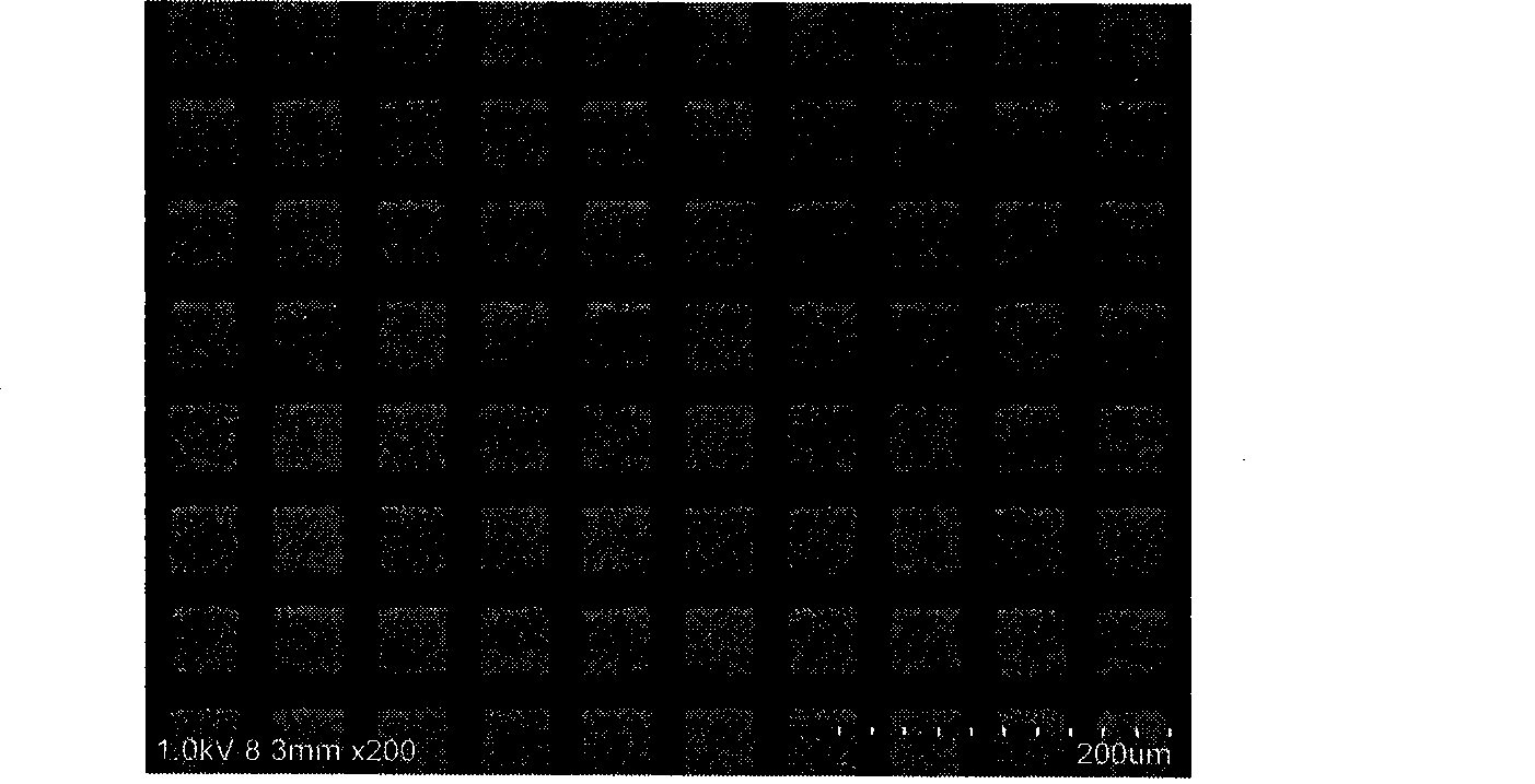
[0050] 3) 4 nanometer titanium metal was thermally evaporated on the quartz substrate using a 400-mesh round-hole copper mesh as a mask. The vapor-deposited titanium was heated in a muffle furnace at 600°C in air for 2 hours, cooled to room temperature by natural cooling, and then taken out to obtain a patterned titanium dioxide mask. The scanning electron microscope picture is as follows: Figure 9 shown.

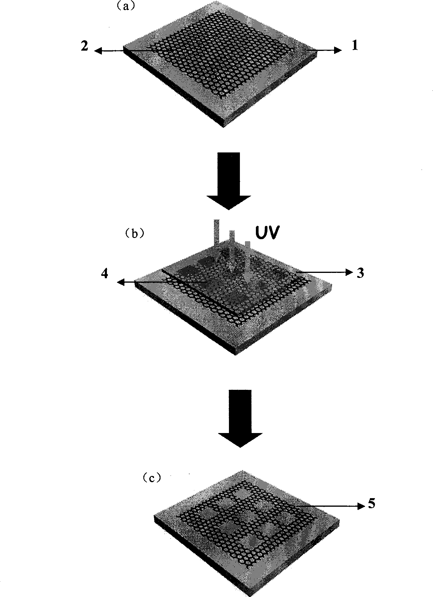
[0051] 4) Contacting the obtained titanium dioxide photomask with the graphene sheet. A xenon light source equipped with an ultraviolet filter was used for illumination for 120 minutes, and the humidity was controlled at 55% (±5%). The patterned graphene can be obtained by removing the titanium dio...


PUM


Abstract

The invention discloses a method for cutting graphene by using titanium dioxide through photocatalysis. The method comprises the steps: 1) a graphene lamellar layer is prepared on a substrate; 2) a convex titanium dioxide nano structure layer is constructed on a quartz substrate to obtain titanium dioxide mask; 3) the titanium dioxide nano structure layer of the titanium dioxide mask is contacted with the graphene lamellar layer and irradiated by ultraviolet light, and the titanium dioxide mask has photocatalysis reaction under the irradiation of the ultraviolet light and can simultaneously cut the graphene to obtain patterned graphene. The method avoids the use of solution phase, has high efficiency and mild reaction condition, and is not limited by the substrate, thus being compatible with the existing semiconductor technique and laying foundation for the development of graphene surface flexible electronic devices.

Description

technical field [0001] The invention relates to a method for tailoring and modifying nanometer material structures, in particular to a method for cutting graphene by means of titanium dioxide photocatalysis, and belongs to the technical field of graphene cutting. Background technique [0002] Graphene has a stable two-dimensional lattice structure and excellent electrical properties, and has rapidly become a "star molecule" in the family of carbon materials in recent years. Due to its compatibility with traditional silicon semiconductor processes and the lack of selective growth faced by carbon nanotubes, graphene shows broad application prospects in the field of nanoelectronic devices and is expected to become the core material for the next generation of electronic devices. . [0003] The shape of graphene sheet determines its energy band structure, which in turn determines its electrical properties, which in turn determine its application. At present, a major challenge f...

Claims


Application Information

Patent Timeline
IPC IPC(8): B82B3/00B01J21/06C01B31/02
Inventor 刘忠范张黎明
Owner PEKING UNIV
Why Eureka
Try Eureka