Gallium nitride based LED epitaxial substrate and preparing process thereof

A light-emitting diode, gallium nitride-based technology, applied in the direction of electrical components, circuits, semiconductor devices, etc., can solve the problems of difficult control of the manufacturing process, high equipment and process requirements, and insignificant increase in reflectivity, etc., to achieve easy manufacturing process The control and preparation methods are simple and diverse, and the effect of reducing production costs

Inactive Publication Date: 2009-08-12
HANGZHOU SILAN AZURE
View PDF5 Cites 25 Cited by
  • Summary
  • Abstract
  • Description
  • Claims
  • Application Information

AI Technical Summary

Problems solved by technology

[0002] Gallium nitride-based light-emitting diodes commonly used in the world are mainly heteroepitaxy on a flat substrate, where the substrate can be sapphire, silicon carbide or silicon. The main disadvantages of this structure are: 1. Since there is no lattice matching GaN-based light-emitting diodes are grown on substrates such as sapphire, silicon carbide, or silicon. The difference in lattice constants causes many dislocations in the epitaxial materials. These defects limit the light-emitting diodes. 2. When light enters the substrate from the epitaxial layer, because the interface is relatively flat, the incident angle of light is relatively small, and the refractive index difference between gallium nitride and the substrate is not large, resulting in low reflectivity, and most of the light will Escape to the substrate and cannot be effectively reflected back to the epitaxial layer, which greatly reduces the light extraction efficiency of GaN-based light-emitting diodes, especially the refractive index of the substrate of GaN-based blue-green light-emitting diodes with silicon carbide as the substrate. Gallium Nitride is comparable, 100% chance of light escaping from the epitaxial layer to the substrate
[0004] 1. Since the refractive index of sapphire is 1.8, which is relatively close to that of gallium nitride, when light enters the graphics substrate from the epitaxial layer, the reflectivity does not increase significantly, and the improvement of the light output rate of GaN-based light-emitting diodes is not as expected Effect
[0005] 2. Since the sapphire substrate is relatively hard, the production process has high requirements on equipment and technology, especially the dry etching of sapphire requires a helium cooling system and high-density plasma. Ordinary etching equipment cannot meet the requirements. Similarly, wet etching requires the use of strong acid at high temperature, and the production process is difficult to control, resulting in low yield and increased production costs.

Method used


Image

  • Gallium nitride based LED epitaxial substrate and preparing process thereof
  • Gallium nitride based LED epitaxial substrate and preparing process thereof
  • Gallium nitride based LED epitaxial substrate and preparing process thereof

Examples


Embodiment Construction

[0030] The following examples illustrate the preparation method of gallium nitride-based light-emitting diode epitaxial substrates,

[0031] Embodiment 1 of the preparation method of gallium nitride-based light-emitting diode epitaxial substrate includes the following steps:

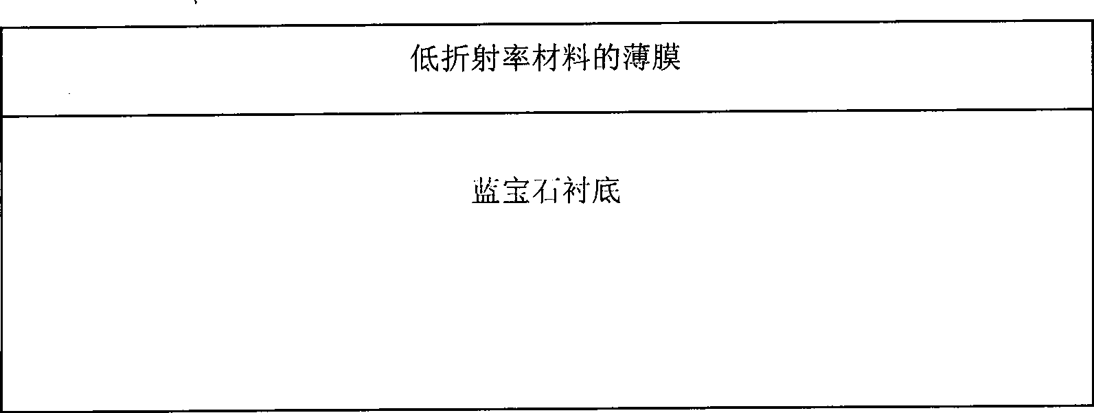
[0032] (1) On a 2-inch C-plane sapphire substrate, a 1.5um silicon dioxide film is grown by chemical vapor deposition, such as figure 1 shown;

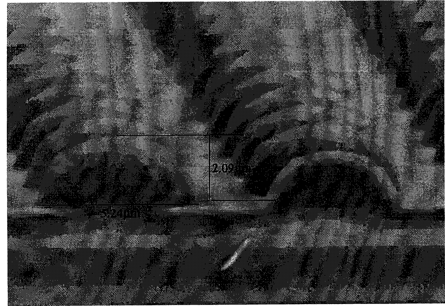
[0033] (2) Prepare a hemispherical mask on the silicon dioxide film with photoresist, such as figure 2 shown;

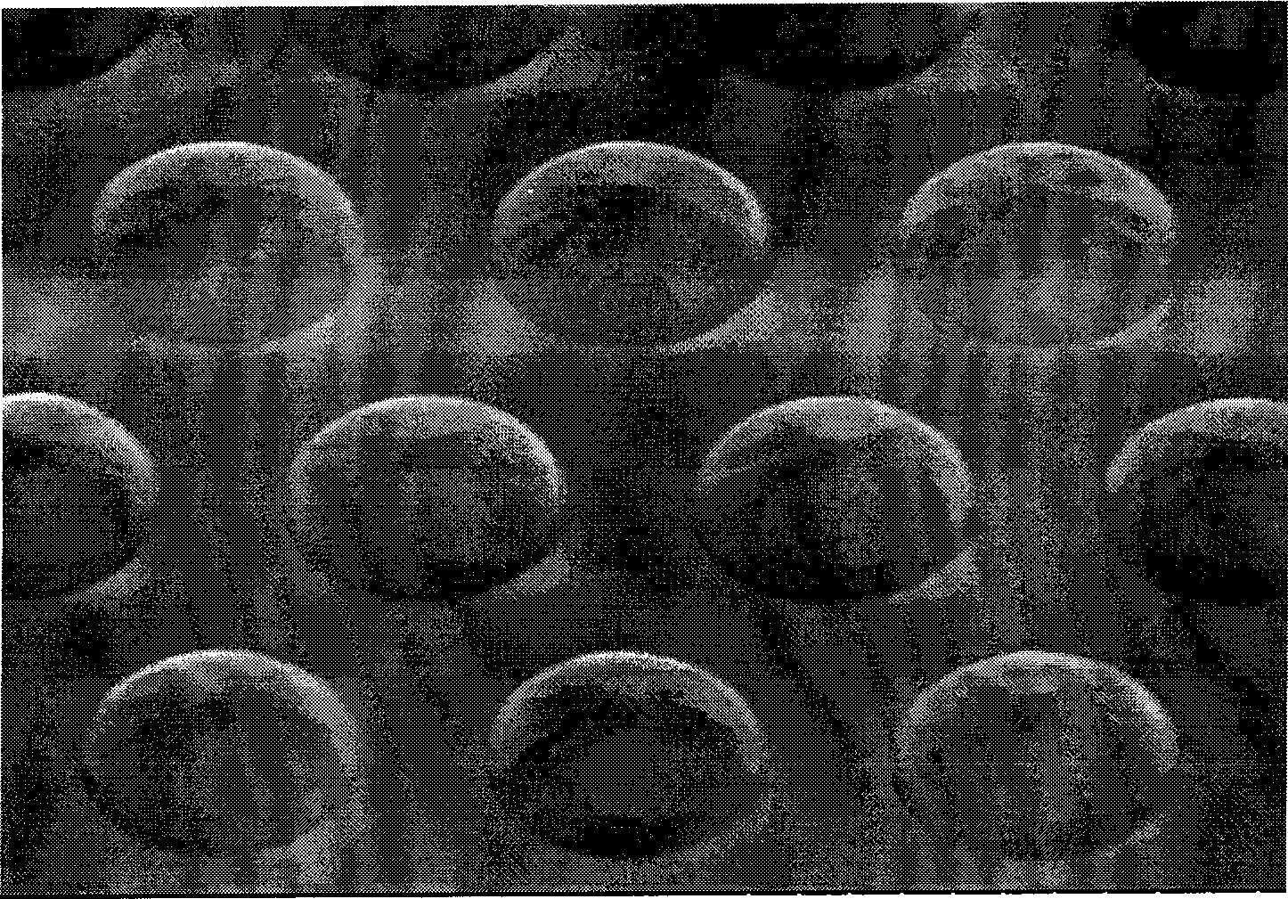
[0034] (3) By dry etching, the hemispherical photoresist mask pattern is transferred to the silicon dioxide film, and the hemispherical silicon dioxide is formed on the sapphire substrate, and the silicon dioxide material between the hemispheres is etched clean , exposing the sapphire substrate.

[0035] (4) Use No. 3 solution (H at 150 degrees Celsius) 2 SO 4 :H 2 o 2 =3:1) cleaning the sapphire substrate to prepare a sapphire pattern substra...


PUM

PropertyMeasurementUnit
refractive indexaaaaaaaaaa

Abstract

The invention provides a gallium nitride based light-emitting diode epitaxial substrate and a method for preparing the same. The method comprises the following steps: (1) depositing a layer of film made of a low-refractive-index material; (2) preparing a mask graph on the film by using a photoresist; (3) transferring patterns of a photoresist mask to the film through etching; and (4) cleaning the substrate to remove the residual photoresist, wherein the substrate is one of sapphire, silicon, silicon carbide, gallium arsenide and zinc oxide, the film is one of the materials of silicon dioxide, silicon nitride, silicon oxynitride or titanium dioxide and the like, the thickness of the film is between 0.1 micro-millimeter and 3 micrometers, the refractive index of the film is less than 2.5, and the substrate pattern is approximately semispherical, conical or round platform shaped. By adopting the gallium nitride based light-emitting diode epitaxial substrate, the light-emitting efficiency of a diode can be improved, the preparation process is easy to control, the preparation method is simple and various, the yield is high, and the production cost is reduced.

Description

technical field [0001] The invention relates to a gallium nitride (GaN)-based light-emitting diode (LED) and a preparation method thereof, in particular to a gallium nitride-based light-emitting diode (LED) epitaxial substrate and a preparation method thereof. Background technique [0002] Gallium nitride-based light-emitting diodes commonly used in the world are mainly heteroepitaxy on a flat substrate, where the substrate can be sapphire, silicon carbide or silicon. The main disadvantages of this structure are: 1. Since there is no lattice matching GaN-based light-emitting diodes are grown on substrates such as sapphire, silicon carbide, or silicon. The difference in lattice constants causes many dislocations in the epitaxial materials. These defects limit the light-emitting diodes. 2. When light enters the substrate from the epitaxial layer, because the interface is relatively flat, the incident angle of light is relatively small, and the refractive index difference betwe...

Claims


Application Information

Patent Timeline
Patent Type & Authority Applications(China)
IPC IPC(8): H01L33/00
Inventor 江忠永徐瑾陈立人李东升田洪涛杨辉张向飞
Owner HANGZHOU SILAN AZURE
Why Eureka
Try Eureka