

Method for preparing substrate having monocrystalline film
A technology of single crystal thin film and single crystal substrate, which is applied in semiconductor/solid-state device manufacturing, electrical components, circuits, etc., can solve problems such as economic disadvantages, high material costs and process costs, safety and health issues, and achieve low cost , high smoothness, less crystal defects
- Summary
- Abstract
- Description
- Claims
- Application Information
AI Technical Summary
Problems solved by technology
Method used
Image

Examples
Embodiment 1
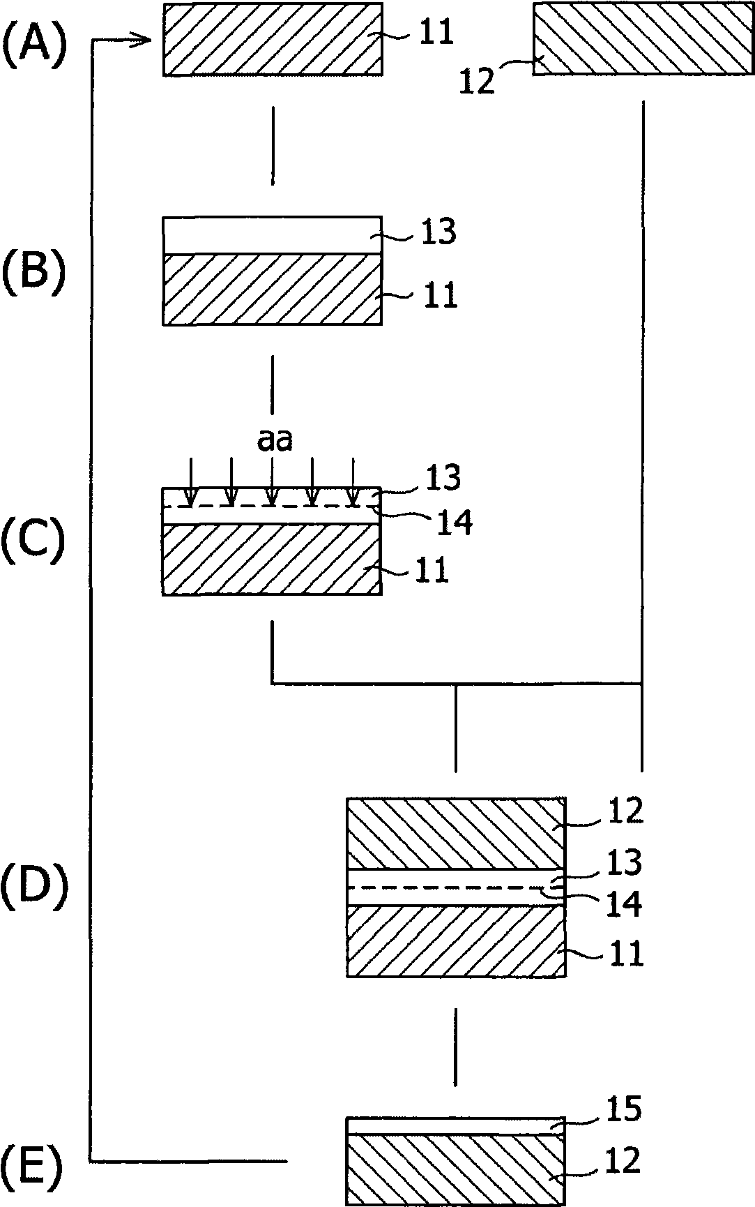
[0060] according to figure 1 The steps shown prepare a substrate with a diamond film.
[0061] exist figure 1 In the step (A), silicon single crystal substrates having a diameter of 6 inches (150 mm) and a thickness of 625 μm were provided as the donor substrate 11 and the handle substrate 12 . The surface roughness (Ra) of the prepared processing substrate 12 was 0.3 nm as measured by using an atomic force microscope (AFM).
[0062] exist figure 1 In the step (B), the donor substrate 11 is placed in a 2.45GHz microwave plasma device, and plasma CVD is carried out under the conditions of 30Torr (4,000Pa) and 850° C. hydrogen. As a result, the diamond layer 13 grew to a thickness of 15 μm.
[0063] exist figure 1 In the step (C), the dosage is 5×10 17 / cm 2 Hydrogen ions were implanted into the diamond layer 13 grown on the donor substrate 11, so that an ion-implanted layer 14 was formed at a depth of 500 nm from the surface.
[0064] exist figure 1 In the step (D), t...
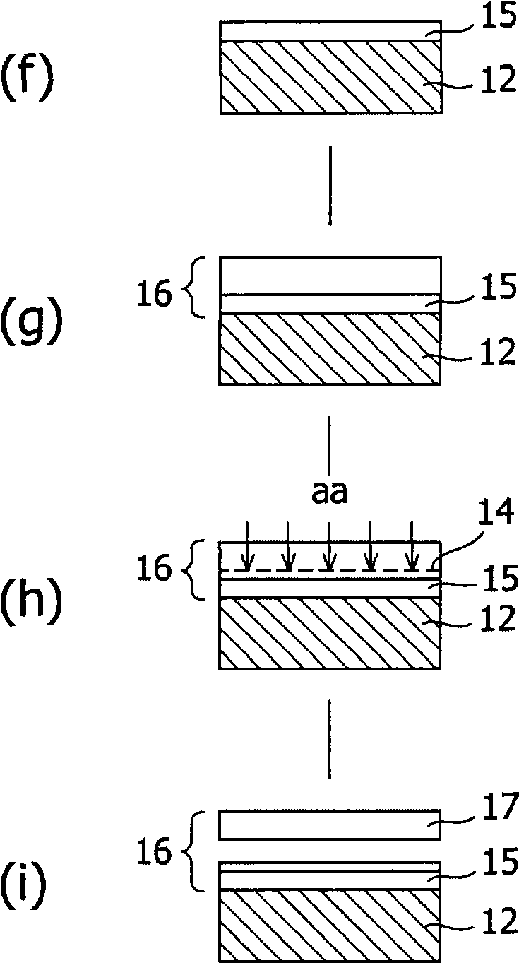
Embodiment 2
[0069] exist figure 1In step (A) of , a synthetic quartz substrate having a diameter of 4 inches (100 mm) and a thickness of 400 μm was provided as a donor substrate 11 . An AlN buffer layer with a thickness of 1 μm was stacked by reactive sputtering on a synthetic quartz substrate. A sapphire substrate having a diameter of 4 inches (100 mm) was provided as the handle substrate 12 . The surface roughness (Ra) of the processed substrate 12 was 0.38 nm as measured by using an atomic force microscope (AFM).
[0070] exist figure 1 In step (B) of , by the HVPE (Hydride Vapor Phase Epitaxy) method, using ammonia water and gallium chloride, in the presence of hydrogen gas as a carrier gas, at 1,050°C under atmospheric pressure, on the donor substrate 11 A GaN single crystal layer 13 with a thickness of 8 μm was grown on the surface of the buffer layer.
[0071] exist figure 1 In the step (C), the dosage is 9×10 16 / cm 2 Hydrogen ions were implanted into the GaN single crystal...
PUM
 Abstract
Description
Claims
Application Information