Silicon-based nanometer column array heterojunction film solar battery and preparation method thereof

A technology of nano-column arrays and solar cells, applied in circuits, electrical components, photovoltaic power generation, etc., can solve the problems of poor masking effect of silicon nanocrystals, technical application of solar cells, corrosion of crystalline silicon nano-columns, etc., and shorten the transportation distance , Improve collection efficiency and reduce the consumption of silicon materials

Inactive Publication Date: 2009-09-02
INST OF MICROELECTRONICS CHINESE ACAD OF SCI
View PDF0 Cites 19 Cited by
  • Summary
  • Abstract
  • Description
  • Claims
  • Application Information

AI Technical Summary

Problems solved by technology

However, this technology has not been applied to the field of solar cells
Moreover, the masking effect of silicon nanocrystals is poor, and they themselves will be etched so that the masking effect cannot be achieved, resulting in undesirable corrosion of crystalline silicon nanopillars, which affects the final battery characteristics

Method used


Image

  • Silicon-based nanometer column array heterojunction film solar battery and preparation method thereof
  • Silicon-based nanometer column array heterojunction film solar battery and preparation method thereof
  • Silicon-based nanometer column array heterojunction film solar battery and preparation method thereof

Examples


Embodiment 1

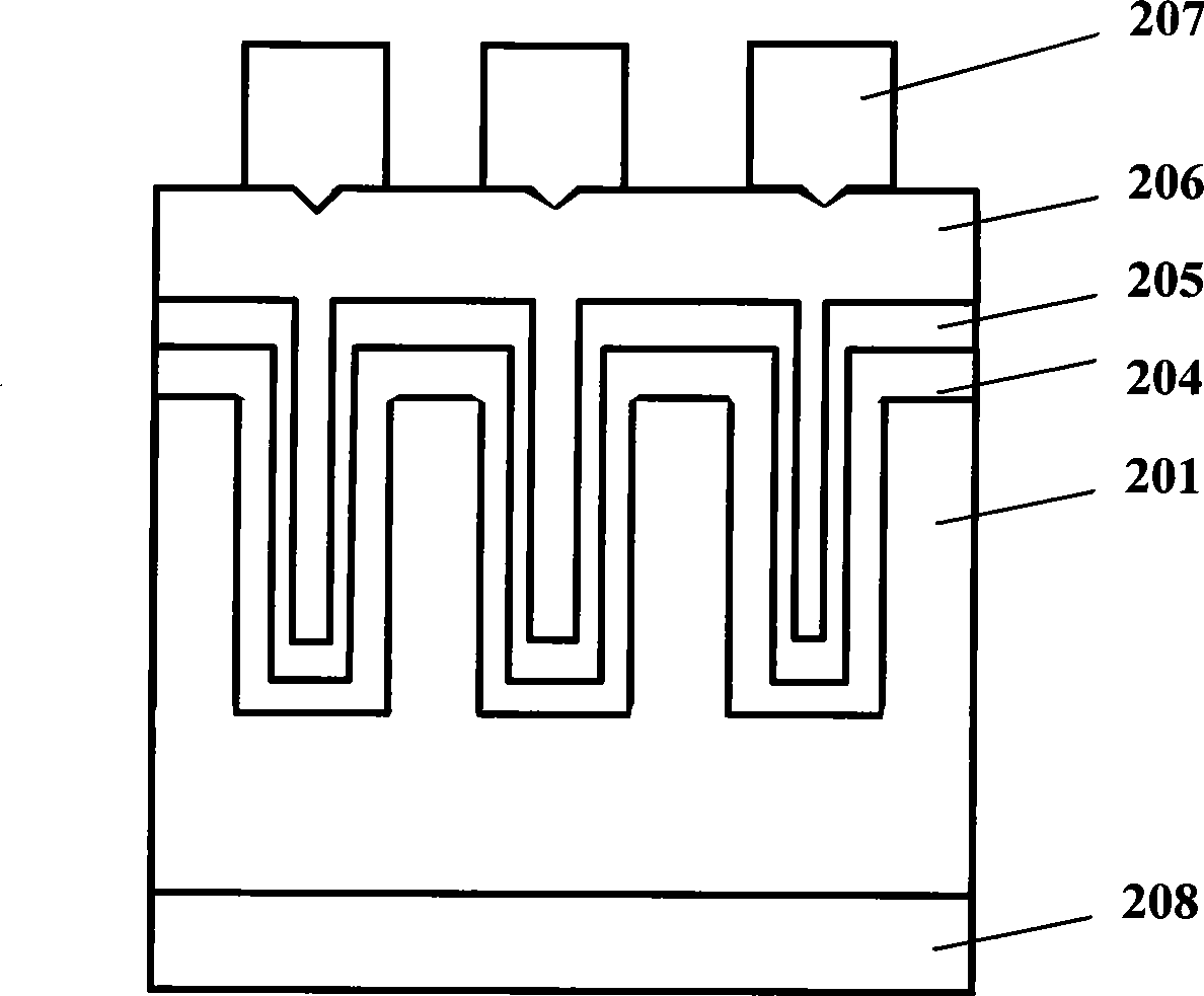
[0043] Such as figure 2As shown, the structure of the silicon-based nanocolumn array heterojunction thin film solar cell of the present invention includes a silicon nanocolumn array 201, an intrinsic amorphous silicon layer 204, an N-type amorphous silicon layer 205, a transparent conductive thin film layer 206, and an upper contact electrode 207 and lower contact electrode 208 .

[0044] The lowermost layer is a vertical silicon nanopillar array 201 . The silicon nanopillar array 201 is one-dimensional nanopillars formed by etching P-type single crystal silicon. The layer is prepared by dry etching technology with Ni nanocrystals as a mask. Since the diameter of the Ni nanocrystal itself is on the order of nanometers, an array of silicon nanopillars with a diameter on the order of nanometers can be obtained.

[0045] An intrinsic amorphous silicon layer 204 and an N-type amorphous silicon layer 205 are sequentially deposited on the silicon nanopillar array 201 . The intr...

Embodiment 2

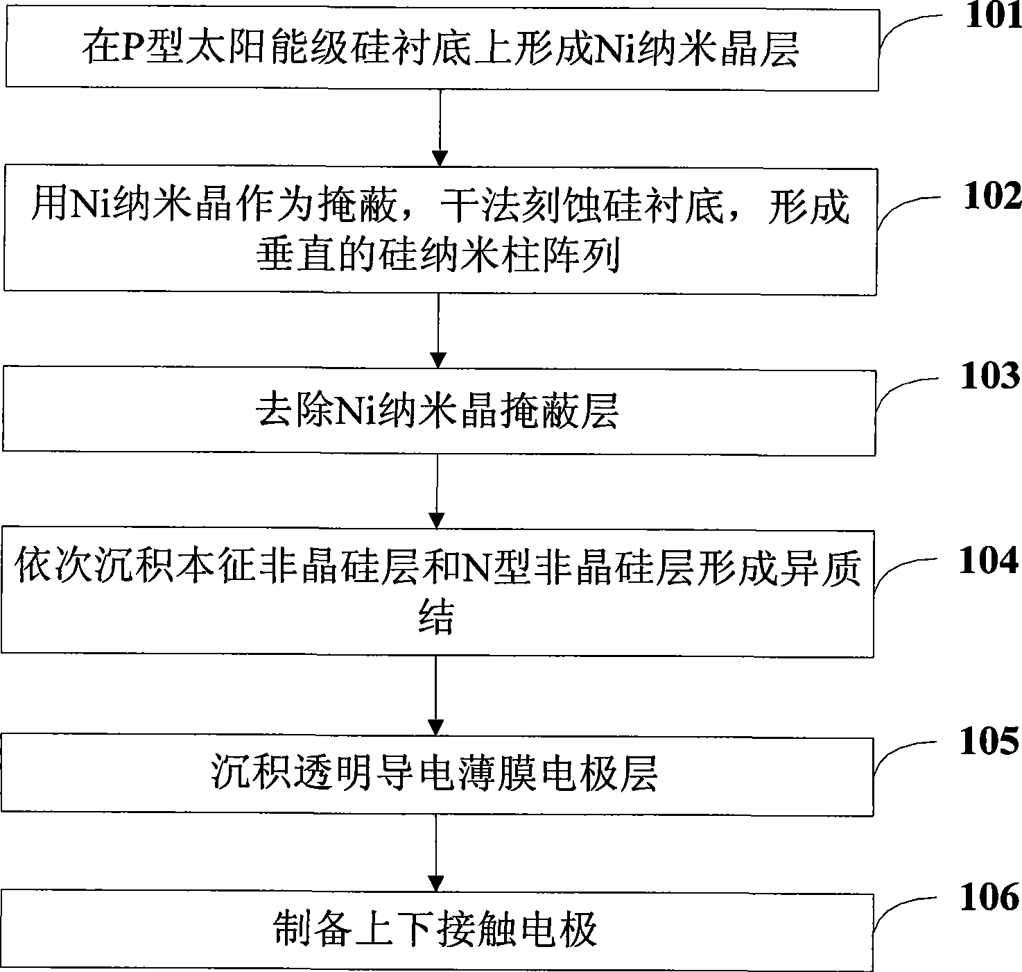
[0049] The invention also discloses a preparation method of the silicon-based nano-column array heterojunction thin-film solar cell.

[0050] Specific steps such as Figure 3 to Figure 9 Shown:

[0051] Step 101: forming a Ni nanocrystal layer on a P-type solar grade silicon substrate.

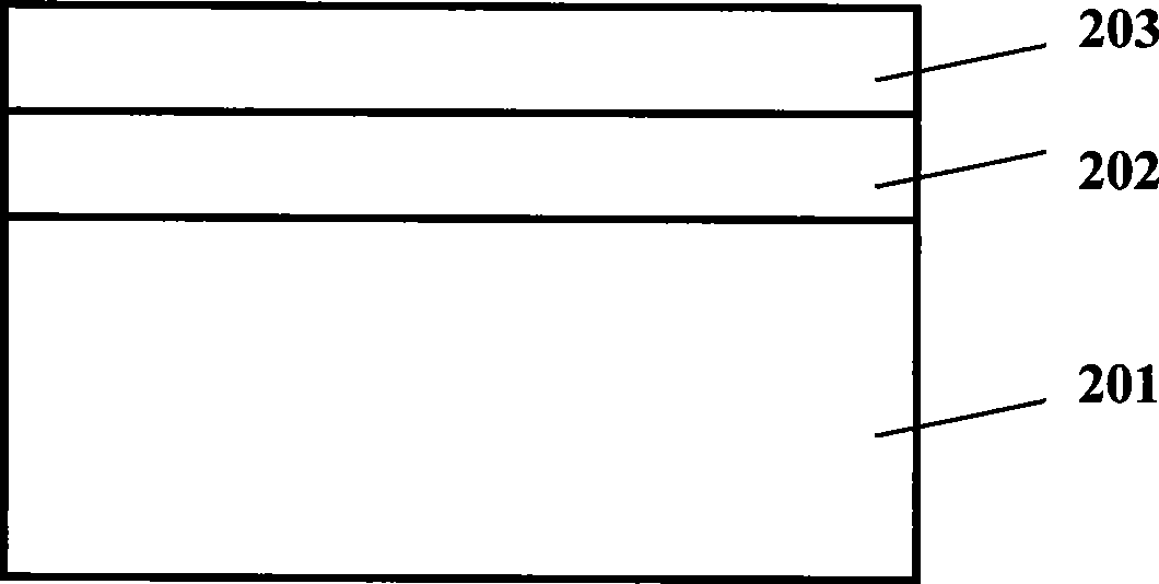
[0052] The selected P-type high-resistance silicon substrate has been diffused and doped with boron (B). The crystal orientation is ; the thickness is 200μm; the resistivity is ρ=3Ωcm -1 .

[0053] Such as image 3 As shown, the P-type solar-grade silicon substrate in this step is a P-type high-resistance silicon substrate after boron (B) diffusion doping. The metallic Ni layer is formed by electron beam evaporation. First, the EVP92 electron beam vacuum coating system is used on the silicon substrate 201 and the natural oxide layer 202, and the vacuum degree is 1.1×10 -6 Below Torr, the metal Ni layer was evaporated at room temperature. The thickness is preferably 2-3nm, and the evapo...


PUM

PropertyMeasurementUnit
thicknessaaaaaaaaaa
thicknessaaaaaaaaaa
thicknessaaaaaaaaaa

Abstract

The invention discloses a silicon-based nanometer column array heterojunction film solar battery and a preparation method thereof, belonging to the field of solar battery manufacture. The method comprises the following steps: preparing a metal nanocrystalline masking layer on a P-type solar silicon substrate; using the metal nanocrystalline masking for masking, adopting a dry method to erode the silicon substrate and preparing a silicon nanometer column array; removing the metal nanocrystalline masking; sequentially depositing an intrinsic amorphous silicon layer and an N-type amorphous silicon layer and forming heterojunction; and finally, depositing a transparent conductive film layer and preparing an upper contact electrode and a lower contact electrode. The method can once prepare a solar battery array with a large area, greatly decreases the cost, has the advantages of simple preparation technology, low cost, favorable preparation efficiency and technological stability, has technological flows fully compatible with the preparation technology of the prior crystal silicon solar batteries and film silicon solar batteries and is easy to popularize on a large scale.

Description

technical field [0001] The invention relates to the field of solar cell manufacturing, in particular to a silicon-based nanocolumn array heterojunction thin-film solar cell and a preparation method thereof. Background technique [0002] Since the birth of the first monocrystalline silicon homogeneous PN junction solar cell in 1954, silicon-based solar cells have gone through two stages: the first generation of solar cells represented by crystalline silicon and polycrystalline silicon, and the first generation of solar cells represented by amorphous silicon thin films. Represents the second generation of solar cells. However, traditional silicon-based solar cells based on homogeneous PN junction technology have highlighted problems such as high cost, low efficiency, and serious environmental pollution. [0003] Existing crystalline silicon solar cells generally use wire cutting technology to obtain silicon wafers with a substrate thickness of 25um to 300um. Including the lo...

Claims


Application Information

Patent Timeline
Patent Type & Authority Applications(China)
IPC IPC(8): H01L31/042H01L31/20
CPCY02E10/50Y02P70/50
Inventor 陈晨贾锐朱晨昕李维龙李昊峰张培文赵盛杰刘明
Owner INST OF MICROELECTRONICS CHINESE ACAD OF SCI
Why Eureka
Try Eureka