Method for fabricating light-emitting diode (LED) chip

A technology of light-emitting diodes and manufacturing methods, which is applied in semiconductor devices, electrical components, circuits, etc., can solve problems such as laser burning to the GaN layer, photoelectric parameter changes, lattice mismatch, etc., and achieve the effect of optimizing photoelectric parameters

Inactive Publication Date: 2009-10-07
EPILIGHT TECH +1
View PDF0 Cites 43 Cited by
  • Summary
  • Abstract
  • Description
  • Claims
  • Application Information

AI Technical Summary

Problems solved by technology

[0003] Figure 1a , 1b It is a process for forming a traditional light-emitting diode chip. On a sapphire substrate 14, an N-type nitride layer 13, a P-type nitride layer 11, and a multi-quantum layer between the N-type nitride layer 13 and the P-type nitride layer 11 are grown. After the well layer 12 is etched to expose the N-type layer 13 by an etching process, the N-electrode 20 and the P-electrode 10 are fabricated. After the back grinding and thinning, laser scribing is used, and then the light-emitting diode chip is obtained by splitting with a splitter. The splitting process of the splitter In the above, the crack extends from the sapphire substrate 14 to the contact surface of the sapphire substrate 14 and the N-type nitride layer 13, however, based on the heteroepitaxial structure of the nitride layer on the sapphire substrate 14, it has a large Lattice mismatch, there is a large stress, when the crack reaches the contact surface, it cannot crack along the predetermined direction, and when the crack cracks along the epitaxial layer, it will lead to the generation of bad light-emitting diode chips
The shape of the light-emitting diode chip obtained by this method is irregular, the yield rate is low, and the edge of the chip is rough.
[0004

Method used


Image

  • Method for fabricating light-emitting diode (LED) chip
  • Method for fabricating light-emitting diode (LED) chip
  • Method for fabricating light-emitting diode (LED) chip

Examples


Embodiment Construction

[0017] The preferred embodiments of the present invention are given below in conjunction with the accompanying drawings to describe the technical solution of the present invention in detail.

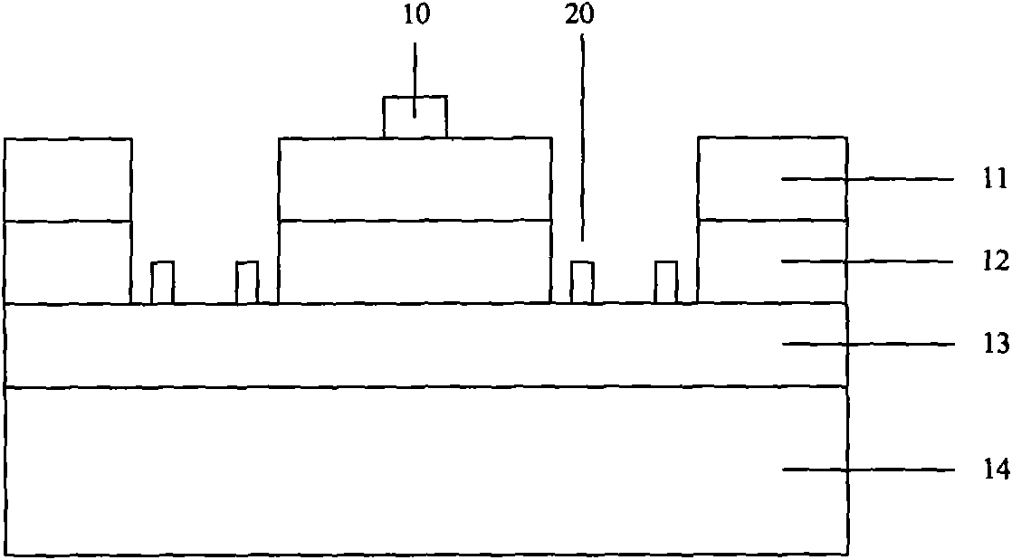
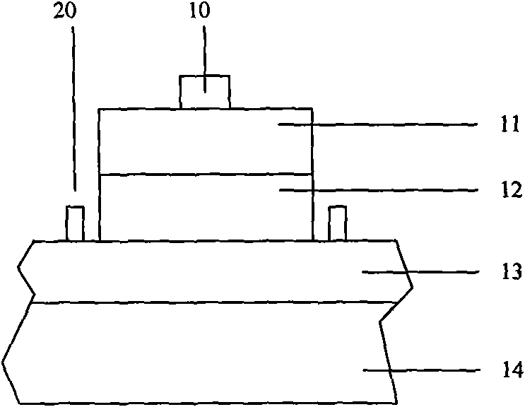
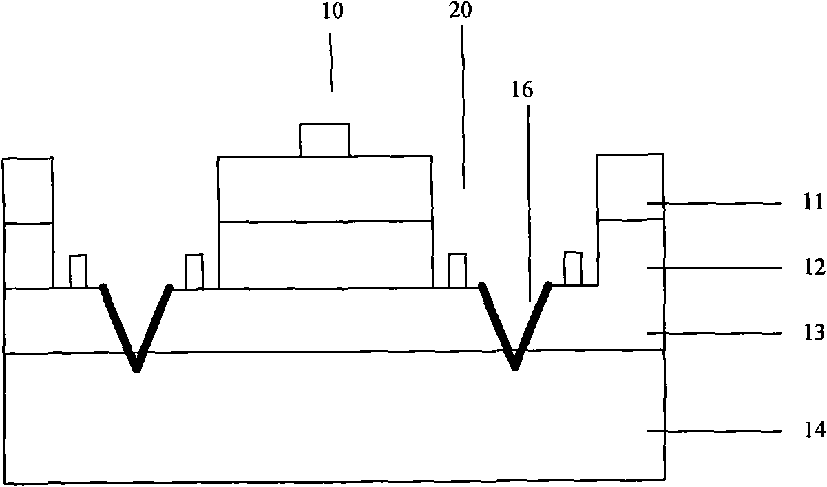
[0018] Please refer to Figure 3a , Figure 3a It is a schematic cross-sectional view of a light-emitting diode wafer in this embodiment. The light-emitting diode wafer includes a sapphire substrate 14 with a thickness of 420um-450um, and an N-type nitride layer 13 and a P-type nitride layer 11 grown on the sapphire substrate 14. And the multi-quantum well layer 12 between the N-type nitride layer 13 and the P-type nitride layer 11. Among them, the growth method of growing the nitride layer on the sapphire substrate 14 is preferably metal organic vapor phase growth method (MOCVD or MOVPE), and molecular beam epitaxy growth method (MBE), halogen vapor phase growth method (Halide VPE), liquid phase growth method can also be used. Growth method (LPE), and different growth methods can also...


PUM


Abstract

The invention provides a method for fabricating light-emitting diode (LED) chip. The method comprises the following steps: (1) forming a N type nitride layer and a P type nitride layer on a sapphire substrate and a multiquantum trap layer between the N type nitride layer and the P type nitride layer to obtain a LED wafer; (2) performing right side scribing to the LED wafer by laser irradiation technology until scribing in to the substrate; (3) etching the LED wafer in the step (2) by etching technology and fabricating a N electrode and a P electrode; (4) performing back side grinding, thinning and splitting to the LED wafer in the step (3) to obtain the LED chip. In the invention, the right side scribing is performed before fabrication of the N and P electrode; the melted level generated in the laser irradiation cutting formation and the residues deposited on the LED wafer side and the surface electrode are removed by the etching process in the fabrication of N and P electrode; thereby, the photoelectric parameter of the chip and the yield rate of the LED chip are optimized.

Description

technical field [0001] The invention relates to a method for manufacturing a light-emitting diode chip, in particular to a method for cutting a GaN epitaxial wafer based on a sapphire substrate into a light-emitting diode chip. Background technique [0002] GaN-based III-V nitrides are an important wide-bandgap semiconductor material with a direct bandgap. Due to its unique bandgap range, excellent optical and electrical properties, and excellent physical and chemical properties, it can be used in blue and green , violet, ultraviolet and white light-emitting diodes, short-wavelength laser diodes, ultraviolet detectors, power electronic devices and other optoelectronic devices and electronic devices, as well as semiconductor devices under special conditions, have been widely used. At present, the sapphire substrate is one of the most commonly used substrates for the epitaxial growth of heterogeneous GaN light-emitting diodes. The nitride-based light-emitting diode wafer is ob...

Claims


Application Information

Patent Timeline
IPC IPC(8): H01L33/00
Inventor 张楠朱广敏郝茂盛张国义陈志忠齐胜利田鹏飞李士涛袁根如陈诚
Owner EPILIGHT TECH
Why Eureka
Try Eureka