

Light emitting diode chip structure and manufacturing method thereof
A light-emitting diode and chip structure technology, which is applied in the direction of electrical components, circuits, semiconductor devices, etc., can solve the problems of increased controllability, limited brightness improvement, long corrosion time, etc., to improve quality and luminous efficiency, reduce interface Reflection, reduce the effect of internal absorption
- Summary
- Abstract
- Description
- Claims
- Application Information
AI Technical Summary
Problems solved by technology
Method used
Image

Examples
Embodiment 1
[0040] Step 1: Make a metal layer on the sapphire by using an electron beam evaporation machine or sputtering, and the metal material is one of titanium and nickel;
[0041] Step 2: Use photoresist to form a layer of photoresist film on the sapphire substrate, the thickness of the film layer is 0.1-2um, use photolithography technology to pattern the photoresist on the substrate to form the desired pattern ; Such as cylinder, round platform, etc.
[0042] Step 3: Reflow the photoresist at low temperature with a rubber baking table, reflow the previous photoresist pattern into a convex hull or truncated cone structure, and reflow the incomplete peripheral graphics caused by the mask operation into a convex hull or truncated cone shape , to make up for the lack of consistency between the peripheral graphics and the central graphics after the mask, so that the graphics consistency on the entire substrate is greatly improved. Reflow conditions: the baking temperature is 100 ° C, an...
Embodiment 2
[0052] Step 1: Make a metal layer on the sapphire by using an electron beam evaporation machine or sputtering, and the metal material is one of aluminum and chromium;
[0053] Step 2: Use photoresist to form a layer of photoresist film on the sapphire substrate, the thickness of the film layer is 5um, and use photolithography technology to pattern the photoresist on the substrate to form the desired pattern;
[0054] Step 3: Reflow the photoresist at low temperature with a rubber baking table, reflow the previous photoresist pattern into a convex hull or truncated cone structure, and reflow the incomplete peripheral graphics caused by the mask operation into a convex hull or truncated cone shape , to make up for the lack of consistency between the peripheral graphics and the central graphics after the mask, so that the graphics consistency on the entire film is greatly improved. Reflow conditions: baking temperature is 50 ° C ~ 250 ° C, time is 10 ~ 60 minutes;
[0055] Step 4...
Embodiment 3
[0064] Step 1: Use photoresist to form a layer of photoresist film on the sapphire substrate, the thickness of the film layer is 0.1um~5um, use photolithography technology to pattern the photoresist on the substrate to form a periodic arrangement the pit;
[0065] Step 2: Evaporate a metal layer on the surface of the previous substrate by electron beam evaporation or sputtering, the metal is nickel or other metals, and the thickness is 0.1-0.5um;
[0066] Step 3: Clean the photoresist by wet cleaning or stripping;
[0067] Step 4: By using metal as a mask, the metal pattern is transferred to the substrate by dry etching.
[0068] Step 5: Clean the metal with wet cleaning, and the corrosion solution is sulfuric acid and nitric acid solution;
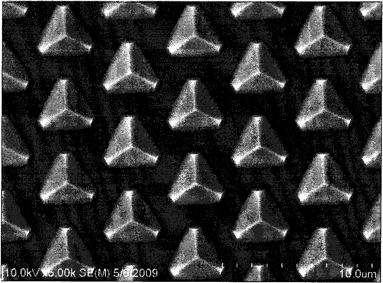
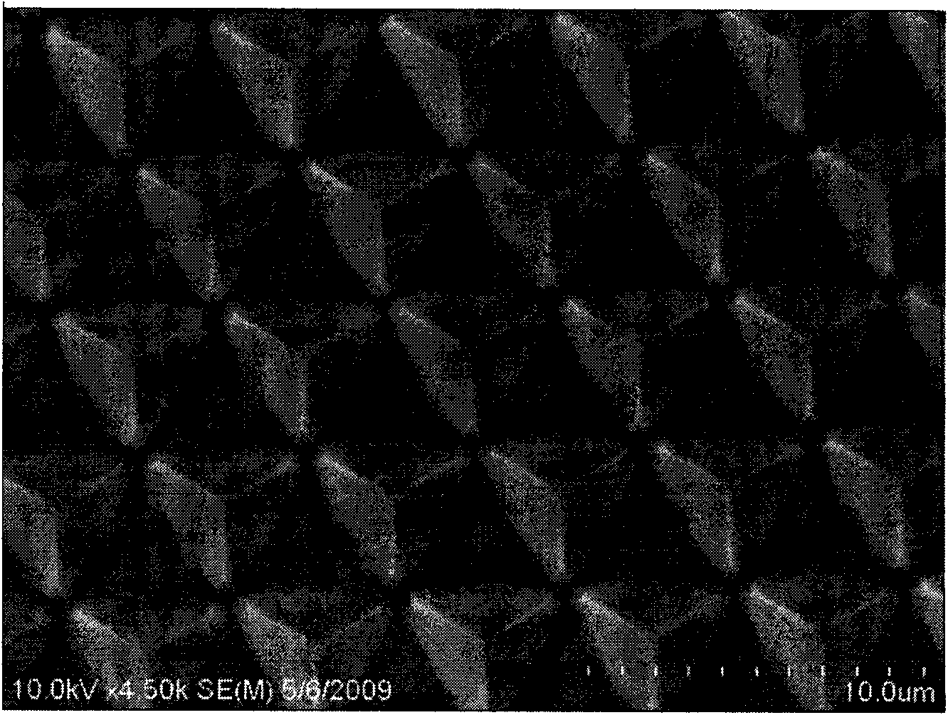
[0069] Step 6: Etching the substrate by a wet method, corroding the pattern after step 1) into a triangular pyramid shape, and the etching solution is a mixed solution of sulfuric acid, phosphoric acid, sulfuric acid and phosphoric acid...
PUM
 Abstract
Description
Claims
Application Information