Photoelectric conversion device and method for manufacturing the same

A photoelectric conversion device and manufacturing method technology, applied in photovoltaic power generation, final product manufacturing, sustainable manufacturing/processing, etc., which can solve the problems of solar cell reliability concerns, inability to simultaneously achieve high productivity, and low productivity

Inactive Publication Date: 2009-12-02
SEMICON ENERGY LAB CO LTD
View PDF5 Cites 6 Cited by
  • Summary
  • Abstract
  • Description
  • Claims
  • Application Information

AI Technical Summary

Problems solved by technology

Therefore, there is a problem that the productivity of a photoelectric conversion device using microcrystalline silicon is lower than that of a photoelectric conversion device using amorphous silicon.
[0011] In the aforementioned Patent Document 1, crystalline silicon (microcrystalline silicon is exemplified) with uniform crystallinity and film properties is formed by controlling the pulse modulation of the high-frequency plasma CVD method. However, compared with the production of amorphous silicon, film formation Slow, so not practical
In addition, in the above-mentioned Patent Document 2, an increase in the film formation rate is sought, but a silicon layer whose thickness is several digits higher than that of amorphous silicon is required, and the problem of productivity cannot be solved.
Therefore, at present, the improvement of characteristics such as high efficiency and the improvement of productivity cannot be achieved at the same time, and the penetration rate of photoelectric conversion devices using silicon thin films cannot reach that of bulk photoelectric conversion devices.
[0012] In addition, in the method of bonding a single crystal silicon substrate and other substrates using the paste for electrode formation as an adhesive as in the above-mentioned Patent Document 3, the degree of adhesion of the adhesive part and the electrode formation as an adhesive Deterioration of paste (decrease in adhesive strength) is a problem, and there is concern about the reliability of the completed solar cell

Method used


Image

  • Photoelectric conversion device and method for manufacturing the same
  • Photoelectric conversion device and method for manufacturing the same
  • Photoelectric conversion device and method for manufacturing the same

Examples


Embodiment approach 1

[0069] One of the features of one aspect of the present invention is that the semiconductor layer exhibiting photoelectric conversion includes crystals in an amorphous structure, and the crystals penetrate between a pair of impurity semiconductor layers joined to form an internal electric field. In this embodiment, a photoelectric conversion device in which a plurality of unit elements are stacked is shown. When one aspect of the present invention is applied to a tandem or stacked type photoelectric conversion device, the layer exhibiting photoelectric conversion as at least one unit element is applied to an amorphous structure including penetration A crystalline semiconductor layer between a pair of impurity semiconductor layers joined to form an internal electric field.

[0070] figure 1 A schematic diagram showing a unit element according to an aspect of the present invention. A unit element according to an aspect of the present invention has a structure in which a semiconduc...

Embodiment approach 2

[0124] In this embodiment, a photoelectric conversion device having a structure different from the above-mentioned embodiment is shown. Specifically, it shows the number of stacked unit elements and figure 2 Different examples of photoelectric conversion devices.

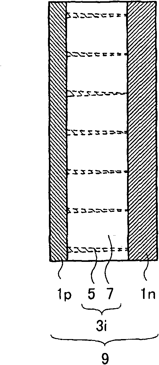
[0125] Figure 5A A single junction type photoelectric conversion device having one unit cell is shown. The photoelectric conversion device includes a unit element 40 composed of a p-type semiconductor impurity semiconductor layer 41p, an i-type semiconductor semiconductor layer 43i, and an n-type semiconductor impurity semiconductor layer 41n laminated on a substrate 2 on which the first electrode 4 is formed. And the second electrode 6 formed on the unit element 40, and includes at least one semiconductor junction. In the semiconductor layer 43i, crystals 45 are dispersed in the amorphous structure 47. In addition, the crystal 45 penetrates the semiconductor layer 43i between the impurity semiconductor layer 41p and...

Embodiment approach 3

[0129] In this embodiment, a photoelectric conversion device having a structure different from the above-mentioned embodiment is shown. Specifically, an example in which a low-concentration impurity semiconductor layer of the same conductivity type as the impurity semiconductor layer of the one conductivity type is formed at a junction of an impurity semiconductor layer of one conductivity type and an intrinsic semiconductor layer is shown.

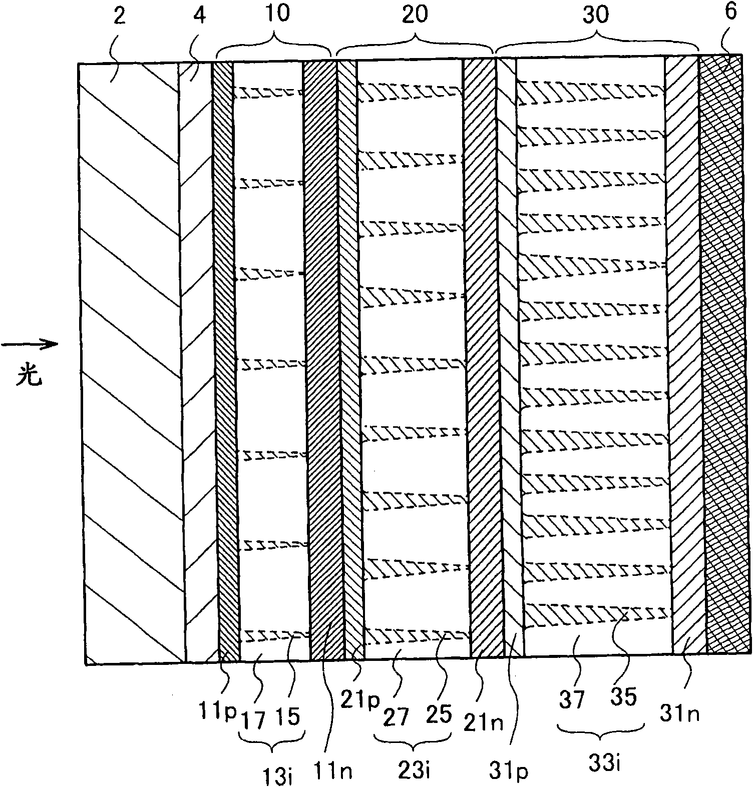
[0130] Figure 6A to 6C A stacked photoelectric conversion device in which three unit elements are formed is shown. in Figure 6A In this case, the first unit element 10, the second unit element 20, the third unit element 30, and the second electrode 6 are arranged from the side of the substrate 2 on which the first electrode 4 is formed. Impurity semiconductor layer 11p, first low-concentration impurity semiconductor layer 12p - , The first semiconductor layer 13i and the second impurity semiconductor layer 11n, the second unit element 20 i...


PUM


Abstract

The object of the present invention is to realize high efficiency and improved productivity at the same time. A photoelectric conversion device comprises a unit having a semiconductor structure, the unit comprises: a conductive first impurity semiconductor layer; a conductive second impurity semiconductor layer reverse to the conductive first impurity semiconductor layer; and a semiconductor layer comprising a crystal region over the first impurity semiconductor layer and the second impurity semiconductor layer in an amorphous structure. The flow ratio of the dilution gas is set more than 1 time and less than 10 times of the semiconductor material gas, preferably setting more than 1 time and less than 6 times, and leading in a reaction space to generate plasma to form a semiconductor layer comprising a crystal region.

Description

Technical field [0001] The invention relates to a photoelectric conversion device with a semiconductor junction and a method for manufacturing the photoelectric conversion device. Background technique [0002] In order to cope with the global environmental problems in recent years, the market for photovoltaic conversion devices represented by solar cells such as residential solar power generation systems has been expanding. Bulk photoelectric conversion devices using monocrystalline silicon or polycrystalline silicon with high photoelectric conversion efficiency have been put into practical use. Photoelectric conversion devices using single crystal silicon or polycrystalline silicon are manufactured by dividing them from large silicon ingots. However, it takes a long time to manufacture a large silicon ingot, so its productivity is not high. Moreover, due to the limitation of the supply of silicon raw materials, it cannot cope with the expansion of the market and is in a state of...

Claims


Application Information

Patent Timeline
Patent Type & Authority Applications(China)
IPC IPC(8): H01L31/04H01L31/042H01L31/0376H01L31/0352H01L31/20H01L31/0725
CPCH01L31/1804H01L31/202H01L31/0725Y02E10/50H01L31/03529Y02E10/547Y02E10/548Y02P70/50H01L31/04
Inventor 山崎舜平
Owner SEMICON ENERGY LAB CO LTD
Why Eureka
Try Eureka