Method for preparing hydrogenated silicon film by utilizing magnetron sputtering

A magnetron sputtering coating and magnetron sputtering technology, applied in the direction of sputtering coating, ion implantation coating, metal material coating process, etc., can solve aggregation, Si-Si bond breaking, movement and density increase, etc. Problems, to achieve the effect of smooth surface, good compactness, and increase crystallization rate

Inactive Publication Date: 2010-03-03
XI AN JIAOTONG UNIV
View PDF0 Cites 16 Cited by
  • Summary
  • Abstract
  • Description
  • Claims
  • Application Information

AI Technical Summary

Problems solved by technology

However, the introduction of H atoms also brings some adverse effects, such as the diffusion of H atoms in the film, which easily causes the breakage of weak Si-Si bonds and the aggregation of H, resulting in the movement of defects and the increase of density.

Method used


Image

  • Method for preparing hydrogenated silicon film by utilizing magnetron sputtering
  • Method for preparing hydrogenated silicon film by utilizing magnetron sputtering
  • Method for preparing hydrogenated silicon film by utilizing magnetron sputtering

Examples


Embodiment 1

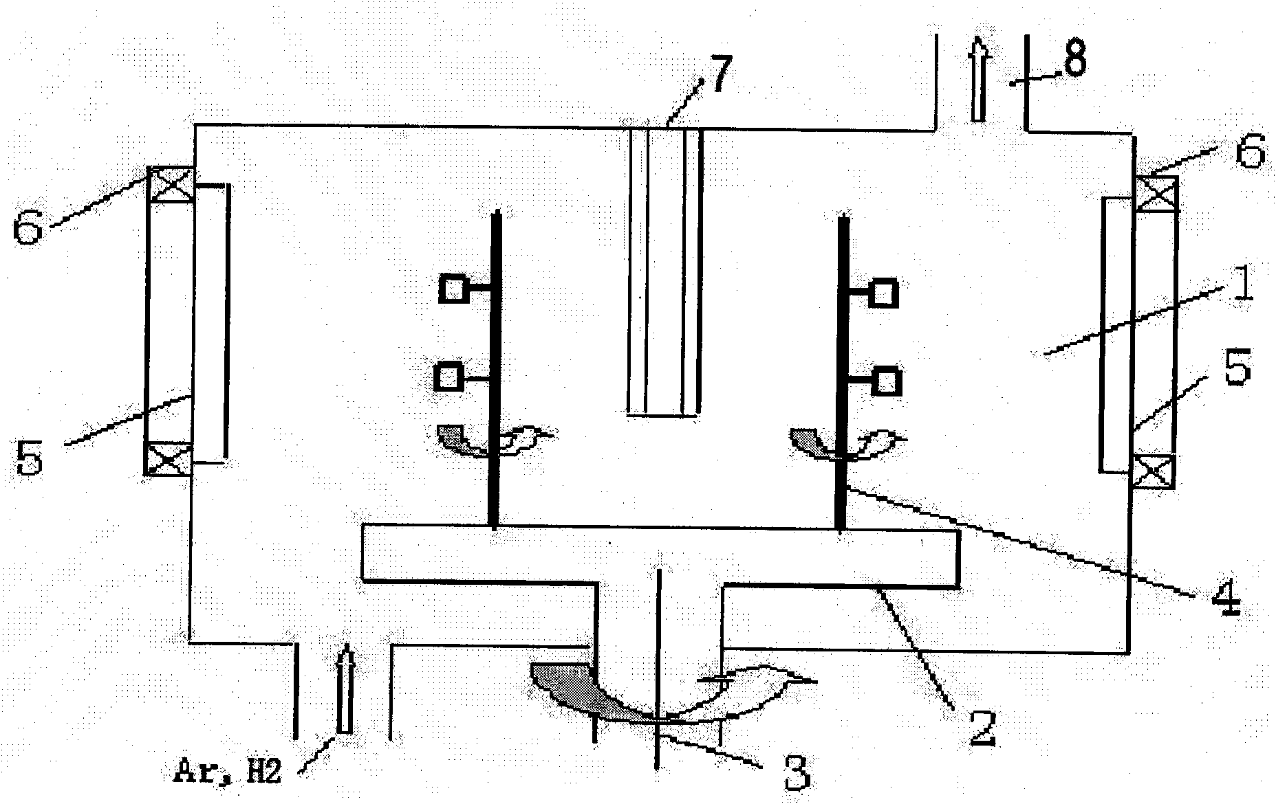
[0030] Evacuate the air pressure of the vacuum chamber to 6×10 -3 Pa, heat the common glass sheet to 250°C; before coating, pass 16sccm of Ar into the vacuum chamber 1 in the furnace, when the pressure in the vacuum chamber reaches 6Pa and keep the pressure stable at 6Pa, open the bias voltage from 3 to -1000V The vacuum chamber and the substrate are bombarded and cleaned for 30 minutes; this can ensure a better bond between the film and the substrate.

[0031] After the substrate was cleaned, the Ar gas was turned off, and the air pressure in the vacuum chamber was pumped to 6×10 -3 Pa, while feeding Ar gas and H 2 gas to make H 2 The volume percentage of the gas is 60%. When the vacuum chamber pressure rises to 0.5Pa, adjust the negative bias to -100V, turn on the control power of the Si target, adjust the power of the Si target to 2kW, and the deposition time is 120min to obtain hydrogenated silicon. film.

Embodiment 2

[0033] Evacuate the air pressure of the vacuum chamber to 8×10 -4 Pa, heat the quartz glass sheet to 240°C; before coating, pass 24 sccm of Ar into the vacuum chamber 1 in the furnace, when the pressure in the vacuum chamber reaches 8Pa and keeps the pressure stable at 8Pa, open the bias voltage from 3 to -800V The vacuum chamber and the substrate were bombarded and cleaned for 40 min.

[0034]After the substrate was cleaned, the Ar gas was turned off, and the air pressure in the vacuum chamber was evacuated to 8×10 -4 Pa, while feeding Ar gas and H 2 gas to make H 2 The volume percentage of the gas is 20%. When the vacuum chamber pressure rises to 0.3Pa, adjust the negative bias to -100V, turn on the control power of the Si target, adjust the power of the Si target to 4kW, and the deposition time is 60min to obtain hydrogenated silicon. film.

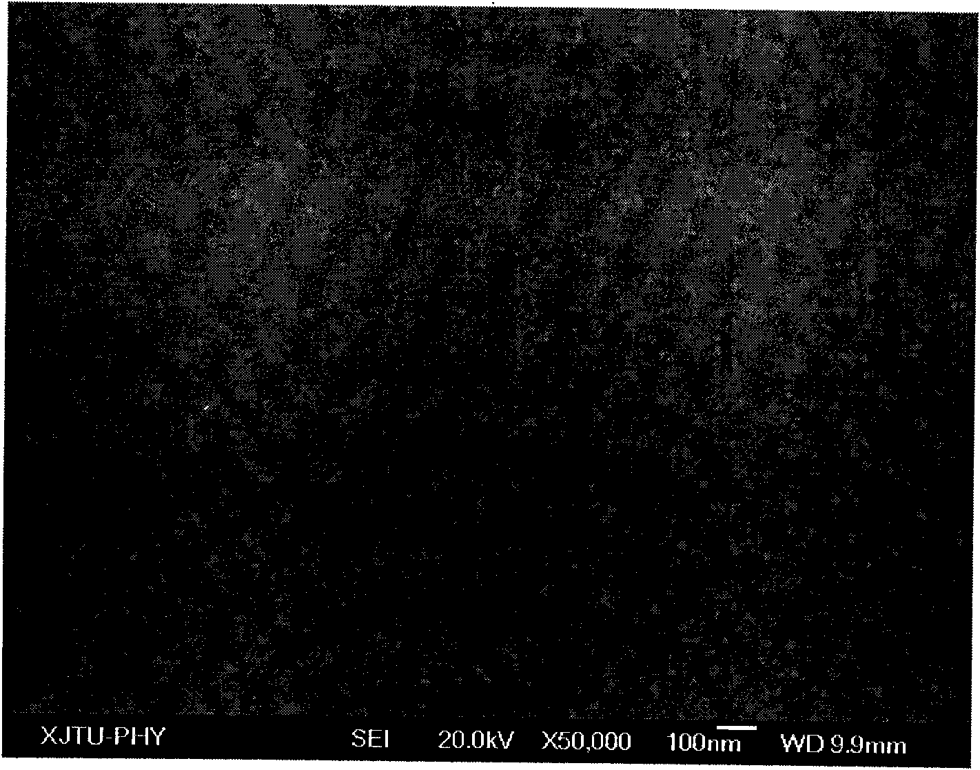
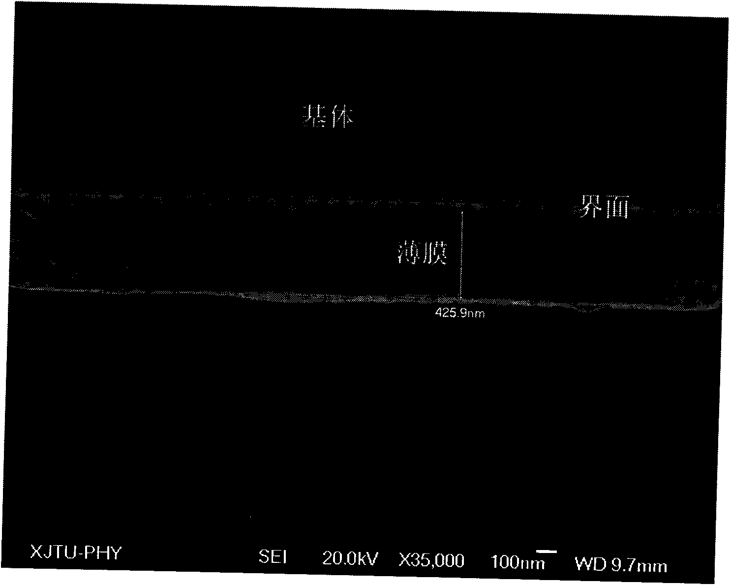
[0035] The thin film grown on the quartz glass plate is vacuum annealed in the later stage to increase the crystallization rate o...

Embodiment 3

[0037] Evacuate the air pressure of the vacuum chamber to 5×10 -3 Pa, heat the single crystal Si(100) sheet to 200°C; before coating, pass 18 sccm of Ar into the vacuum chamber 1 in the furnace, and when the pressure in the vacuum chamber reaches 4Pa and keeps the pressure stable at 4Pa, turn on the bias 3 to -900V to bombard and clean the vacuum chamber and substrate for 20 minutes.

[0038] After the substrate was cleaned, the Ar gas was turned off, and the air pressure in the vacuum chamber was evacuated to 5×10 -3 Pa, while feeding Ar gas and H 2 gas to make H 2 The volume percentage of the gas is 40%. When the vacuum chamber pressure rises to 0.4Pa, adjust the negative bias to -100V, turn on the control power of the Si target, adjust the power of the Si target to 3kW, and the deposition time is 90min to obtain hydrogenated silicon. film.

[0039] The thin film grown on the single crystal silicon wafer is vacuum annealed in the later stage to increase the crystallizati...


PUM

PropertyMeasurementUnit
thicknessaaaaaaaaaa
thicknessaaaaaaaaaa
particle sizeaaaaaaaaaa

Abstract

The invention discloses a method for preparing a hydrogenated silicon film by utilizing magnetron sputtering. The method comprises the following steps, pretreating a substrate and placing the substrate in a magnetron sputtering filming device; utilizing a plane Si target as a source of Si element; adjusting the power of an intermediate frequency pulse power supply to control the sputtering rate ofthe Si target; utilizing high-purity Ar gas as main ionization gas, and ensuring the effective glow discharge process; and adopting high-purity H2 gas as reaction gas, ionizing the H2, and combiningthe H2 with the Si element, forming the hydrogenated silicon film on the surface of the substrate through deposition, and annealing the film at the temperature of 550 DEG C to 950 DEG C in vacuum to obtain the nano-crystalline/non-crystalline composite structure. The invention achieves regulation and control to microstructure of the hydrogenated silicon film by changing introduction proportion ofhydrogen so as to further change the photoelectric properties of the film. The preparation method is simple and reliable, and the prepared hydrogenated silicon film is hopeful to be applied to solar batteries.

Description

technical field [0001] The present invention relates to the preparation of thin film materials, in particular to a method for preparing a silicon hydrogenated thin film on a single crystal Si (100) sheet, a quartz glass sheet and an ordinary glass sheet substrate. The silicon hydrogenated thin film prepared by the method has an adjustable microstructure , the characteristic that the energy band gap can be changed is expected to be widely used in solar cell materials. Background technique [0002] In recent years, solar energy has attracted widespread attention as a clean energy source, and a solar cell is a device that directly converts sunlight energy into electrical energy. Today, silicon solar cells dominate the solar cells. At present, crystalline silicon solar cells have been industrialized, but the shortage and high price of silicon raw materials limit the wide application of crystalline silicon solar cells. Therefore, solar cells based on thin film technology have b...

Claims


Application Information

Patent Timeline
Patent Type & Authority Applications(China)
IPC IPC(8): C23C14/35C23C14/06
Inventor 马胜利王利
Owner XI AN JIAOTONG UNIV
Why Eureka
Try Eureka