Microwave/millimeter wave sensor apparatus

一种传感器装置、毫米波的技术,应用在测量装置、无线电波的反射/再辐射、仪器等方向,能够解决检测灵敏度不利、高RF/IF变换增益、复杂结构等问题,达到实现单纯结构、高效放射特性、高效接收特性的效果

Inactive Publication Date: 2010-03-24
NAT INST OF INFORMATION & COMM TECH
View PDF0 Cites 17 Cited by
  • Summary
  • Abstract
  • Description
  • Claims
  • Application Information

AI Technical Summary

Problems solved by technology

[0007] However, as in the invention described in Non-Patent Document 1, in the structure in which the GUNN diode is directly mounted in the circular conductor patch, although there is no power loss due to the transmission line, the DC / RF conversion efficiency of the GUNN diode itself is different from that of the GUNN diode. Transistors are very poor in comparison, so power consumption increases, and stable operation cannot be expected unless a high heat dissipation structure is adopted
In addition, GUNN diodes cannot expect higher RF / IF conversion gain than transistors, so they are disadvantageous in terms of detection sensitivity.
Furthermore, in the invention described in Non-Patent Document 1, although a planar conductor patch type radiation structure is adopted, a sensor device expected to have a simple structure, low cost, and high power efficiency cannot be realized.
[0008] In addition, as in the invention described in Non-Patent Document 1, an oscillation FET is arranged in the center of two semicircular conductor patches capacitively coupled by a chip capacitor, and a mixing FET is directly mounted in the drain side conductor patch. In the structure of the Schottky barrier diode, since a plurality of RF band parts are arranged in the conductor patch, it has to become a complicated structure
In addition, capacitive coupling using chip capacitors is difficult to achieve in the millimeter wave band, and Schottky barrier diodes are used for frequency mixing, so higher RF / IF conversion gains than transistors cannot be expected. This point of sensitivity is disadvantageous in
[0009] Also, as in the invention described in Non-Patent Document 3, only a microstrip line transistor oscillation circuit designed for a 50Ω load is connected to the feeding point of a square conductor patch antenna designed for a 50Ω load on the same plane. In this case, unavoidable coupling occurs between the square patch antenna and the microstrip conductor of the oscillation circuit, so the conductor pattern of the oscillation circuit affects the radiation output, radiation pattern, and oscillation frequency characteristics
The invention described in Non-Patent Document 3 has such disadvantages that it is difficult to deal with it practically.
Furthermore, the invention described in Non-Patent Document 3 is configured to connect a general microstrip square patch antenna with an input impedance of 50 ohms to a general microstrip line oscillation circuit with an output impedance of 50 ohms, so that the antenna and the oscillation circuit are not separated. Integral, especially in the millimeter wave band, it is disadvantageous in terms of efficiency because the power loss caused by the microwave band part constituting the feedback circuit for oscillation etc. increases

Method used


Image

  • Microwave/millimeter wave sensor apparatus
  • Microwave/millimeter wave sensor apparatus
  • Microwave/millimeter wave sensor apparatus

Examples


no. 1 Embodiment approach

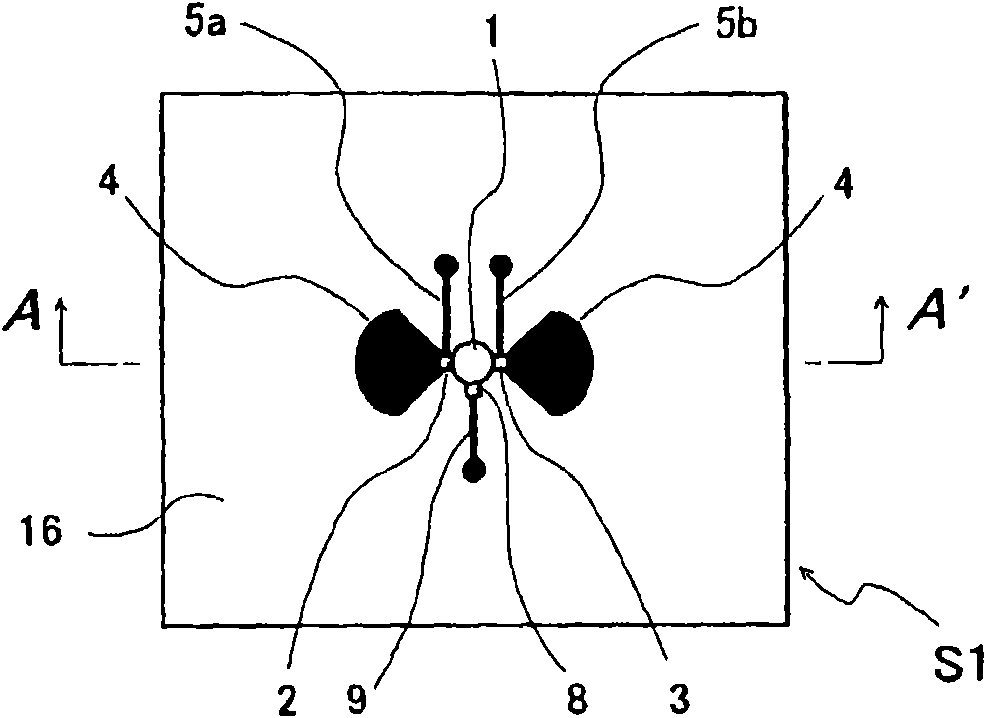
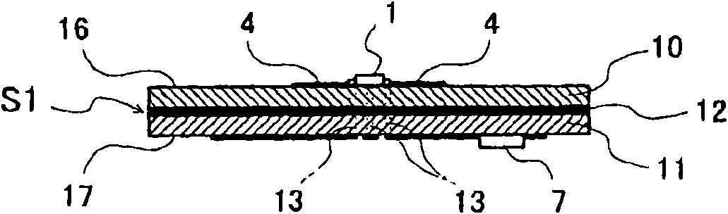
[0096] Figure 1A , Figure 1B , Figure 1C A schematic configuration of the microwave / millimeter wave sensor device according to the first embodiment is shown, Figure 1A is the surface diagram of the radial oscillator substrate S1, Figure 1B yes Figure 1A A cross-sectional view in the arrow direction of line A-A' in FIG. 1C is a rear view of the radial oscillator substrate S1. Radiating oscillator substrate S1 has a three-layer substrate structure in which an inner layer GND 12, which is a ground conductor layer, is interposed between a front-side dielectric substrate 10 and a back-side dielectric substrate 11. The high-frequency transistor 1 of the radiation type oscillator substrate S1 is supplied with DC power, and the detection signal (IF signal) extracted from the radiation type oscillator substrate S1 is processed by the signal analysis processing unit P.

[0097] That is, the radiation oscillator board S1 functions as a "radiation oscillator that integrates three-...

no. 2 Embodiment approach

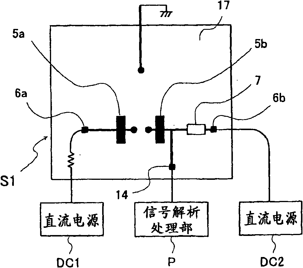
[0118] Figure 5 A circuit configuration diagram of the microwave / millimeter wave sensor device according to the second embodiment is shown. The radiation oscillator substrate S2 is supplied with DC power from the DC power sources DC1 and DC2, and the radiation oscillator substrate S2 is connected to the radiation oscillator substrate S2 through the signal analysis processing unit P. The extracted detection signal (IF signal) is analyzed and processed. The microwave / millimeter wave sensor device of the present embodiment is obtained by changing the extraction position of the IF signal in the microwave / millimeter wave sensor device of the first embodiment. In addition, the same reference numerals are assigned to the same configurations as those of the microwave / millimeter wave sensor device shown in the first embodiment, and description thereof will be omitted.

[0119] In the radial oscillator substrate S2, the source 8 of the high-frequency transistor 1 is connected to the m...

no. 3 Embodiment approach

[0121] Figure 6 A circuit configuration diagram of the microwave / millimeter wave sensor device according to the third embodiment is shown. Direct current power is supplied to the radiation oscillator substrate S3 from the DC power sources DC1 and DC2, and the radiation oscillator substrate S3 is supplied to the radiation oscillator substrate S3 through the signal analysis processing unit P. The extracted detection signal (IF signal) is analyzed and processed. The microwave / millimeter wave sensor device of the present embodiment is obtained by changing the mounting position of the conductor patch 4 in the microwave / millimeter wave sensor device of the first embodiment described above. In addition, the same reference numerals are assigned to the same configurations as those of the microwave / millimeter wave sensor device shown in the first embodiment, and description thereof will be omitted.

[0122] On the radiation oscillator substrate S3, conductor patches 4, 4 are attached ...


PUM


Abstract

A microwave / millimeter wave sensor apparatus can obtain sensitive detected information while attaining a simple constitution, low costs and high efficiency of power. In the sensor apparatus, a planar radiation type oscillator substrate (S1) having an inner layer GND (12) interposed between a front surface side dielectric substrate (10) and a rear surface side dielectric substrate (11) has a pair of conductor patches (4, 4) axisymmetrically on the side of a front surface layer (16). A gate (2) and a drain (3) of a microwave transistor (1) are respectively connected to the conductor patches (4,4) to supply power to the gate (2) and the drain (3) of the microwave transistor (1) by a gate-side RF choke circuit (5a) and a drain-side RF choke circuit (5b). An impedance line (9) satisfying an oscillation condition is connected to a source (8) to transmit a transmission RF signal in an RF zone as a planar radiation type oscillator and to receive a reception RF signal as reflected waves from a matter to be measured, thus obtaining an IF signal as detected information by homodyne mixing.

Description

technical field [0001] The present invention relates to transmitting signals in the microwave / millimeter wave band to an object to be measured, and detecting (such as motion detection, speed detection, presence detection, and position detection, etc.) information related to the object to be measured by receiving reflected waves from the object to be measured Microwave / millimeter wave sensor device. Background technique [0002] Conventional microwave / millimeter wave sensor devices are configured by connecting a transistor oscillator circuit or a GUNN diode oscillator circuit, a diode mixer circuit, an antenna, a coupler, a splitter, and a transmitter / receiver separation device through a transmission line such as a microstrip line. Independent functional circuits such as circulators. In such a conventional microwave / millimeter wave sensor device, the oscillation signal of the oscillation circuit is generally used as a transmission RF signal, and a part of the oscillation sig...

Claims


Application Information

Patent Timeline
Patent Type & Authority Applications(China)
IPC IPC(8): G01S7/03G01S13/04G01S13/931
CPCG01S7/032H03B5/1852H01Q1/2208G01S7/03G01S2013/9378G01S13/931G01S13/87G01S13/34H01Q9/285G01S2013/9375G01S2013/9385H01Q23/00G01S2013/93274G01S2013/93272G01S2013/93271
Inventor 歌川仁史松井敏明
Owner NAT INST OF INFORMATION & COMM TECH
Why Eureka
Try Eureka