UV LED area source for offset printing press and manufacturing method thereof

A surface light source and offset printing machine technology, which is applied to the UV LED surface light source used in offset printing machines and its production field, can solve problems such as uneven irradiation, increased operating costs, and weak luminous intensity, and achieve uniform and stable irradiation, and improved Printing efficiency, effect of reducing curing cost

Inactive Publication Date: 2010-05-12
江苏广发光电科技有限公司
View PDF0 Cites 7 Cited by
  • Summary
  • Abstract
  • Description
  • Claims
  • Application Information

AI Technical Summary

Problems solved by technology

However, due to the need for microwave transmission channels, the electrodeless lamp has a large volume and is expensive.
[0004] (2) Traditional ultraviolet light sources such as iodine-gallium lamps and ultra-high pressure mercury lamps have a large wavelength range, large heat release, and low curing efficiency
The volume of the cooling equipment is often larger than the light source itself, resulting in more auxiliary equipment, complicated operation, and increased operating costs
In addition, the performance of the cooling equipment plays an important role in the normal operation of the light source, and will directly affect the curing effect
[0006] (4) Uneven irradiation
Iodine-gallium lamps, ultra-high-pressure mercury lamps and other traditional ultraviolet light source lamps in the length direction of the lamp tube have weaker luminous intensity than the middle part, which cannot emit light uniformly, and cannot evenly irradiate flat objects, so that the light intensity absorbed by the curing material is different, which affects the curing effect.
[0007] (5) Poor adjustability
The radiation intensity adjustment of traditional ultraviolet light sources such as iodine-gallium lamps and ultra-high-pressure mercury lamps is generally realized by changing the number of lighted lamps in a multi-lamp light source. The corresponding radiation intensity changes between a limited number of values, and the application is not flexible enough.
For example, each position of a curved surface object can only be treated equally "one size fits all", and a fixed ultraviolet light is emitted, resulting in a significant difference in the light intensity absorbed by different positions on the curved surface; UV materials for different irradiation requirements cannot be adjusted according to the material requirements. radiation intensity

Method used


Image

  • UV LED area source for offset printing press and manufacturing method thereof
  • UV LED area source for offset printing press and manufacturing method thereof
  • UV LED area source for offset printing press and manufacturing method thereof

Examples


specific Embodiment approach

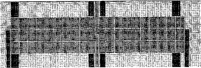
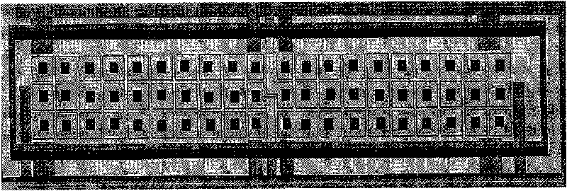
[0018] 1. UV LED surface light source chip fixed substrate

[0019] The UV LED surface light source chip fixing substrate is used to fix high-power LED chips emitting various wavelengths in the 200nm-450nm band, and is a plate-shaped component.

[0020] The main material of the bottom body of the UV LED surface light source chip fixing substrate is aluminum alloy, and other metal materials or composite materials with high thermal conductivity can also be used, such as red copper, ceramics and other materials. The chip fixing position on the UV LED surface light source chip fixing substrate is called a gold bump. The base material of the gold bump is copper, and the surface layer is gold-plated. Other materials with high thermal conductivity can also be used and the surface layer is gold-plated. The role of gold plating on the surface of gold bumps is to effectively increase the bonding effect of high-power LED chips when silver glue is used to bond high-power LED chips. The g...


PUM


Abstract

The invention relates to a UV LED area source for an offset printing press, which is a semiconductor luminous device directly generating ultraviolet light, and belongs to the field of offset printing press printing. The UV LED area source is mainly characterized in that: high-power LED chips of which the luminous wavelength is between 200 and 450nm are integrated in a certain ratio to form the area source or linear source with a certain wavelength in a wave band of which the peak wavelength is between 200 and 450nm; the emission spectrum of the light source is matched with an absorption spectrum of a photosensitizer in a sensitive glue material, namely the length of waves emitted by the UV LED area source is concentrated at the periphery of the absorption wavelength of the photosensitizer so as to effectively improve the absorption rate and highly efficiently trigger the photosensitizer in the sensitive glue; and under the action of the photosensitizer and the ultraviolet light, the glue is combined with the photosensitizer so as to generate a water insoluble solid matter. Because the area source or the linear source is the LED semiconductor light source device, and compared with a supervoltage mercury lamp and a Iodine gallium light, the area source or the linear source cannot cause energy loss caused by infrared light, has extreme low loss and not great temperature rise, avoids the temperature influencing printing materials, and is nontoxic and green; and the area source can be designed into any geometrical shapes such as a linear shape, a surface shape and a three-dimensional shape as required in the actual use. The UV LED area source has strong usability and obvious economic benefit, industry innovation benefit and social benefit.

Description

Technical field [0001] The invention relates to a UV LED surface light source for offset printing machines and a manufacturing method thereof, which emits ultraviolet light of a sensitive wavelength of a photosensitive agent in a photosensitive glue, so that polyvinyl alcohol and a photosensitive agent are combined to produce a water-insoluble solid substance . The spectral peak wavelength of the light source is a specific wavelength in the ultraviolet region and violet region of 200nm to 450nm. Background technique [0002] At present, the ultraviolet light sources used for offset printing are mainly traditional ultraviolet light sources such as iodine gallium lamps and ultra-high pressure mercury lamps. With the wide application in industrial production, traditional UV curing light sources are increasingly exposing some shortcomings: [0003] (1) Traditional ultraviolet light sources such as iodine-gallium lamps and ultra-high-pressure mercury lamps need to be driven by ...

Claims


Application Information

Patent Timeline
Patent Type & Authority Applications(China)
IPC IPC(8): F21S8/00F21V5/00F21V19/00F21V23/00F21V29/00F21V29/02F21Y105/00F21Y101/02F21W131/403F21K9/90F21V29/67F21V29/85F21Y115/10
Inventor 徐志平
Owner 江苏广发光电科技有限公司
Why Eureka
Try Eureka