Micron/nanoscale BiOCl film material and preparation method thereof

A thin-film material, nano-scale technology, applied in metal material coating process, ion implantation plating, coating and other directions, can solve the problems of difficult to homogenize product size and morphology, unfavorable for mass production, and poor product dispersion. , to achieve the effect of uniform morphology, low cost and high yield

Active Publication Date: 2010-06-09
THE NAT CENT FOR NANOSCI & TECH NCNST OF CHINA
View PDF1 Cites 18 Cited by
  • Summary
  • Abstract
  • Description
  • Claims
  • Application Information

AI Technical Summary

Problems solved by technology

The synthesis methods listed above all have the disadvantages of long synthesis period, relatively low yield, difficulty in uniform product size and appearan

Method used


Image

  • Micron/nanoscale BiOCl film material and preparation method thereof
  • Micron/nanoscale BiOCl film material and preparation method thereof
  • Micron/nanoscale BiOCl film material and preparation method thereof

Examples


Embodiment 1

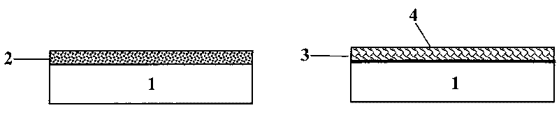
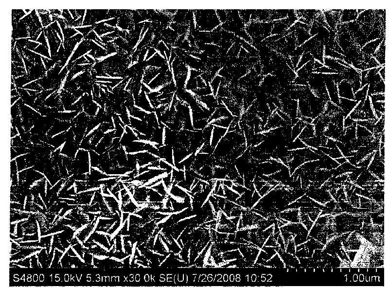
[0035] The micron / nano-scale BiOCl thin film material prepared in this embodiment uses a silicon wafer as the substrate 1, and a layer of metallic bismuth film 2 is deposited on the substrate 1. The metallic bismuth film 2 is used as a raw material to form a layer consisting of two-dimensional The BiOCl thin film 3 composed of BiOCl nanosheets 4; wherein the metal bismuth thin film 2 has a thickness of 200 nm, and the BiOCl thin film has a thickness of 200 nm.

[0036] First use the silicon wafer as the substrate 1, using acetone, alcohol, and deionized water as the cleaning agent, and ultrasonically clean each for 10 minutes. After cleaning, take it out and dry it with nitrogen, then dry it in a vacuum oven at 120°C for 1 hour, and take it out after cooling. . A layer of metallic bismuth thin film 2 is deposited on the silicon wafer treated as above by magnetron sputtering, and the deposition condition: background pressure 1×10 -5 Pa, a sputtering power of 50W, an Ar flow rate o...

Embodiment 2

[0038] The micron / nano-scale BiOCl film material prepared in this embodiment uses a cover glass as the substrate 1, and a layer of metallic bismuth film 2 is deposited on the substrate 1, and the metallic bismuth film 2 is used as a raw material to form a layer consisting of two The BiOCl thin film 3 composed of BiOCl nanosheets 4; wherein the metal bismuth thin film 2 has a thickness of 200 nm, and the BiOCl thin film has a thickness of 200 nm.

[0039] First, the cover glass was used as the substrate 1, and acetone, alcohol, and deionized water were used as the cleaning agent, each ultrasonically cleaned for 10 minutes, and then taken out and dried with nitrogen, then dried in a vacuum oven at 120°C for 1 hour, and then taken out after cooling. Magnetron sputtering is used to deposit metal bismuth film 2 on the cover glass treated as above, and the deposition condition: background pressure 1×10 -5 Pa, sputtering power 50W, Ar flow rate 25sccm, deposition pressure 0.1Pa, substrat...

Embodiment 3

[0041] The micron / nano-scale BiOCl film material prepared in this embodiment uses a conductive transparent glass ITO as the substrate 1, and a metal bismuth film 2 is deposited on the substrate 1. The metal bismuth film 2 is used as a raw material to form a layer of The BiOCl film 3 composed of two-dimensional BiOCl nanosheets 4 has a thickness of 200 nm.

[0042] First, use conductive transparent glass ITO as substrate 1, use acetone, alcohol, and deionized water as cleaning agent, each ultrasonically clean for 10 minutes, then take it out and dry it with nitrogen, then dry it in a vacuum oven at 120°C for 1 hour, and take it out after cooling. . Magnetron sputtering is used to deposit metallic bismuth film 2 on the conductive transparent glass ITO treated as above. The deposition condition: background pressure 1×10 -5 Pa, sputtering power 50W, Ar flow rate 25sccm, deposition pressure 0.1Pa, substrate temperature 250°C, deposition time 600s. Then put the deposited metal bismuth...


PUM

PropertyMeasurementUnit
Thicknessaaaaaaaaaa
Thicknessaaaaaaaaaa

Abstract

The invention relates to a micron/nanoscale BiOCl film material and a preparation method thereof. The film material comprises a substrate. A layer of bismuth metal film is deposited on the substrate; a layer of BiOCl film consisting of two-dimensional BiOCl nano sheets is formed by using the bismuth metal film as a raw material. The thickness of the BiOCl film is between 30nm and 2 mu m. The preparation method for the micron/nanoscale BiOCl film material comprises the following steps: depositing a layer of bismuth metal film on the substrate by adopting physical vapor deposition; soaking in solution containing H2O2 and Cl- by a wet method, adjusting the volume percentage of H2O2 to 1 to 99 percent and the concentration of Cl- to between 0.01 and 2 mol/L to ensure that the pH value of the mixed solution is in a range from 0.5 to 7, keeping the temperature of a reaction system between 20 and 80 DEG C, and soaking for 1 to 60 minutes; and obtaining the micron/nanoscale BiOCl film material with different features after washing. The preparation method for the micron/nanoscale BiOCl film material has the advantages of simple and controllable process, uniform dimension and feature of the product, short production cycle, low cost and suitability for large-scale industrial production. The BiOCl film material has wide application prospects in photocatalysis, optoelectronic thin-film devices, nanocoatings, pearl pigments, and other fields.

Description

Technical field [0001] The invention relates to a V-VI-VII ternary system compound film material and a preparation method thereof, in particular to a BiOCl film material with different micron / nano-scale characteristics and a preparation method thereof. Background technique [0002] Bismuth oxychloride (hereinafter referred to as BiOCl), as a V-VI-VII ternary compound, has unique optical, electrical, magnetic and luminescent properties at the same time. It is used in photocatalysis, photovoltaic thin film devices, nano coatings, pearlescent pigments, etc. The field has broad application prospects. For the nano-scale BiOCl, its large specific surface area and singular properties on the nano-scale make the application prospect of BiOCl more attractive, and it has also attracted the interest of many researchers. The traditional method for preparing general nano-BiOCl materials is to prepare by the hydrolysis precipitation of bismuth nitrate or bismuth chloride in the liquid phase. ...

Claims


Application Information

Patent Timeline
IPC IPC(8): C23C22/58C23C14/22C23C14/18
Inventor 曹四海郭传飞刘前
Owner THE NAT CENT FOR NANOSCI & TECH NCNST OF CHINA
Why Eureka
Try Eureka