

Silicon mask used for super-diffraction photoetching with line width of below 200 nanometers and manufacturing method thereof
A super-diffraction and mask technology, applied in the field of nano-processing, to achieve the effect of convenient mask and manufacturing method, good ultraviolet light blocking, and large depth of pattern layer
- Summary
- Abstract
- Description
- Claims
- Application Information
AI Technical Summary
Problems solved by technology
Method used
Image

Examples
Embodiment 1
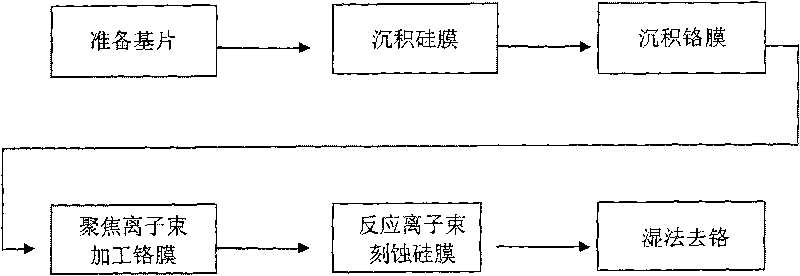
[0026] The first embodiment of the present invention is to make a silicon mask with periodic lines with a period of 100nm and a line width of 50nm. The exposure wavelength is 365nm. The mask includes a transparent quartz substrate and a silicon film pattern on it.
[0027] The mask fabrication steps are as follows figure 1 Shown:
[0028] (1) select quartz material to make ultraviolet light transparent substrate;
[0029] (2) Utilize the magnetron sputtering coating machine to coat a layer of silicon film with a thickness of about 70nm on the transparent quartz substrate;
[0030] (3) Utilize the magnetron sputtering film coater to plate a layer of chromium film with a thickness of 20nm on the upper surface of the silicon film, as a pattern shielding layer in the later etching process;
[0031] (4) Utilize the focused ion beam to directly process the chromium film with a thickness of 20nm, so that periodic nano-line patterns with a period of 100nm and a line width of 50nm ar...
Embodiment 2
[0035] The second embodiment of the present invention is to make a silicon mask with periodic lines with a period of 200nm and a line width of 80nm. The exposure wavelength is 365nm. The mask includes a transparent quartz substrate and a silicon film pattern on it.
[0036] The mask fabrication steps are as follows figure 1 Shown:
[0037] (1) select quartz material to make ultraviolet light transparent substrate;
[0038] (2) utilize a magnetron sputtering coating machine to coat a layer of silicon film with a thickness of about 100 nm on the transparent quartz substrate;
[0039] (3) Utilize the magnetron sputtering film coater to plate a layer of chromium film with a thickness of 30nm on the upper surface of the silicon film, as a pattern shielding layer in the later etching process;
[0040] (4) Utilize the focused ion beam to directly process the chromium film with a thickness of 30nm, so that periodic nano-line patterns with a period of 200nm and a line width of 100nm ...
Embodiment 3
[0044] The second embodiment of the present invention is to make a silicon mask with periodic lines of 64nm and line width of 32nm, and the exposure wavelength is 365nm. The mask includes a transparent quartz substrate and a silicon film pattern on it.
[0045] The mask fabrication steps are as follows figure 1 Shown:
[0046] (1) Select calcium fluoride material to make ultraviolet light transparent substrate;
[0047] (2) Coating a layer of silicon film with a thickness of about 50 nm on the transparent calcium fluoride substrate by using a magnetron sputtering coating machine;
[0048] (3) Utilize the magnetron sputtering film coater to plate a layer of chromium film with a thickness of 10nm on the upper surface of the silicon film, as a pattern shielding layer in the later etching process;
[0049] (4) Utilize the focused ion beam to directly process the chromium film with a thickness of 10nm, so that periodic nano-line patterns with a period of 64nm and a line width of ...
PUM
| Property | Measurement | Unit |
|---|---|---|
| Thickness | aaaaa | aaaaa |
| Wavelength | aaaaa | aaaaa |
| Thickness | aaaaa | aaaaa |
Abstract
Description
Claims
Application Information