

Preparation method of copper and indium alloy ink and application thereof
A copper-indium alloy and ink technology, which is applied in the field of solar energy applications, can solve the problems of difficult nanoparticles and other problems, and achieve the effects of easy dispersion, dense and smooth surface, and large grain size
Inactive Publication Date: 2010-06-16
ZHEJIANG UNIV
View PDF0 Cites 11 Cited by
- Summary
- Abstract
- Description
- Claims
- Application Information
AI Technical Summary
Problems solved by technology
However, because copper particles are more active and easy to oxidize, while indium particles are soft and easy to flatten, it is difficult to obtain nanoparticles with suitable particle size distribution and good dispersion by physical methods.
Method used
View moreImage
Smart ImageViewing Examples

Examples
Embodiment 1
Embodiment 2
Embodiment 3
Login to View More PUM
 Abstract
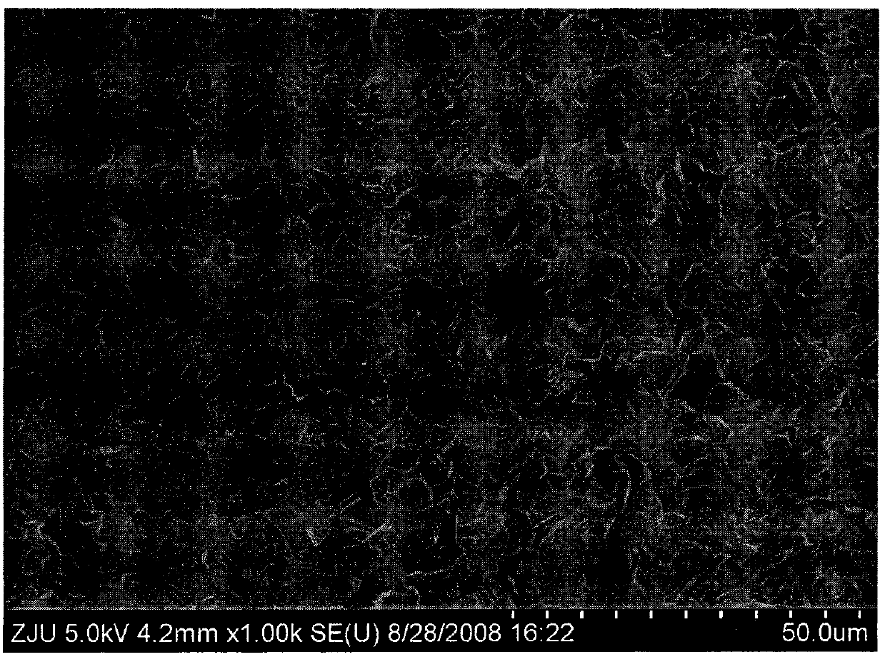
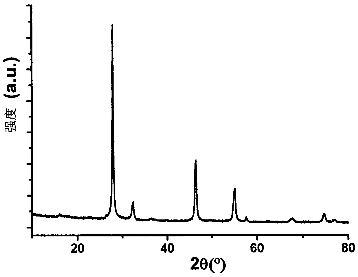
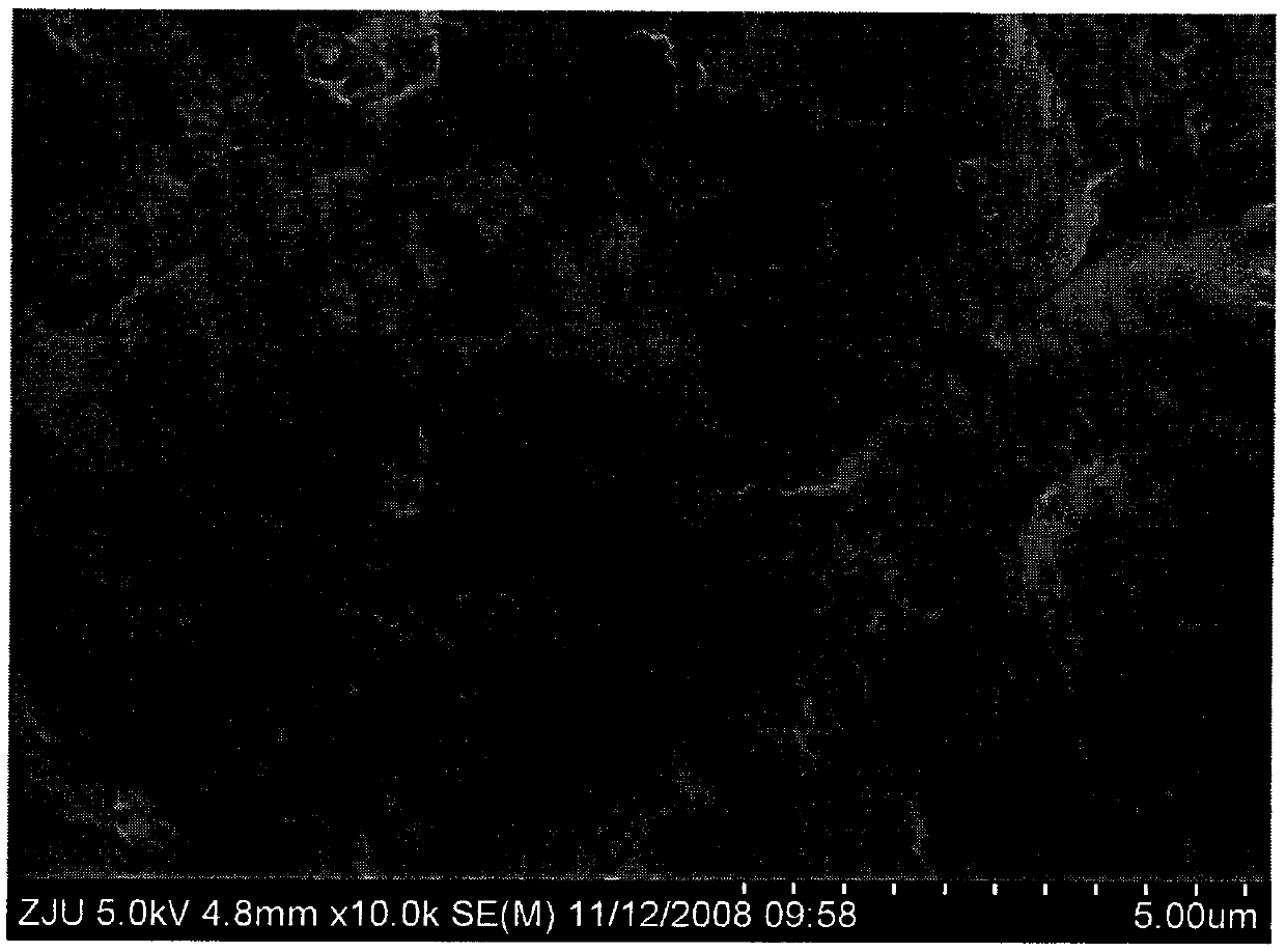
The invention discloses a preparation method of a copper and indium alloy ink, comprising the following steps: (1) dissolving copper chloride and indium chloride in ethylene glycol at 80-200 DEG C, then slowing dropwise adding ethylene glycol solution of sodium borohydride for reaction; carrying out centrifuge, washing and drying to obtain copper and indium alloy nanoparticles; (2) preparing solution according to volume ratio: ethylene glycol: methanol: ethylene glycol methyl ether=2-8: 1:2-6; (2) dispersing the copper and indium alloy nanoparticles obtained in step (1) according to mass ratio: copper and indium alloy nanoparticles : solvent=1 : 2-8 and evenly dispersing the mixture by ultrasonic waves to obtain the copper indium alloy ink. The invention also discloses an application method of the copper and indium alloy ink in preparing sulphur indium copper film or selenium indium copper film. In the invention, a low-cost chemical method is adopted to synthesize copper and indium alloy nanoparticles, the prepared film features compact and smooth surface and large film crystallite dimension after sintering and no obvious film miscellaneous phase.
Description
technical field The invention relates to a preparation method of a copper-indium alloy ink and a method for preparing a sulfur-indium-copper film or a selenium-indium-copper film by using the copper-indium alloy ink, belonging to the field of solar energy applications. Background technique Due to the advantages of low cost and low toxicity of I-III-IV compound semiconductor thin films (mainly sulfur-indium-copper thin films and selenium-indium-copper thin films), they have attracted widespread attention as a new generation of thin-film battery materials. Existing methods for preparing I-III-IV compound semiconductor thin films mainly include: Spray Prolysis, Chemical Vapor Deposition, Molecular Beam Epitaxy, Reactive Sputtering ), vacuum evaporation (single source, dual source, triple source), metal organic chemical vapor deposition (MOCVD), electrodeposition (Elector Deposition), chemical bath method (Chemical Bath Deposition), etc. Some of the above methods need to be app...
Claims
Login to View More Application Information
Patent Timeline
 Patent Type & AuthorityApplications(China)
IPC IPC(8): B22F9/24H01L31/18
CPCY02P70/50
Inventor杨德仁陈官璧汪雷
OwnerZHEJIANG UNIV