Method for preparing enhanced aluminum-gallium-nitrogen/gallium nitride transistor with high electron mobility

A technology with high electron mobility and high mobility, applied in circuits, electrical components, semiconductor devices, etc., can solve the problems of difficult process, high device on-state resistance, high power consumption, etc., and achieve simple process and low on-state High resistance, high reliability effect

Inactive Publication Date: 2010-06-16
INST OF SEMICONDUCTORS - CHINESE ACAD OF SCI
View PDF0 Cites 15 Cited by
  • Summary
  • Abstract
  • Description
  • Claims
  • Application Information

AI Technical Summary

Problems solved by technology

However, due to the extremely low concentration of two-dimensional electron gas in the entire channel, the devices prepared by this method have high on-state resistance and high power consumption, and are not very competitive in applications.
[0006] Inspired by this idea, someone started from the perspective of device technology and used the method of digging to reduce the thickness of the barrier layer directly below the gate electrode, reducing the concentration of two-dimensional electron gas here, and preparing the highest threshold voltage. Enhanced devices with about 0.5 volts have relatively low on-state resistance, but th

Method used


Image

  • Method for preparing enhanced aluminum-gallium-nitrogen/gallium nitride transistor with high electron mobility
  • Method for preparing enhanced aluminum-gallium-nitrogen/gallium nitride transistor with high electron mobility
  • Method for preparing enhanced aluminum-gallium-nitrogen/gallium nitride transistor with high electron mobility

Examples


Embodiment Construction

[0037] In order to make the object, technical solution and advantages of the present invention clearer, the present invention will be described in further detail below in conjunction with specific embodiments and with reference to the accompanying drawings.

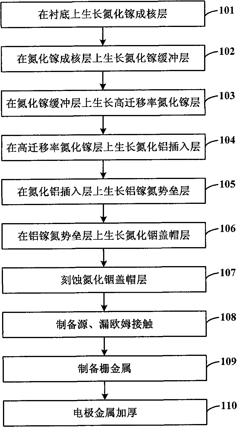
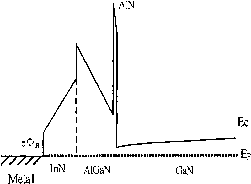
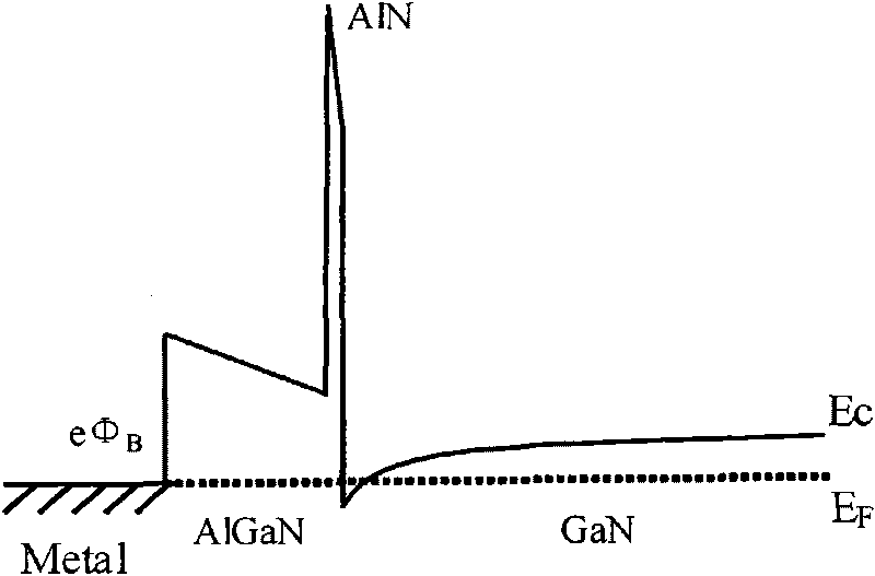
[0038] The enhanced aluminum gallium nitride / gallium nitride high electron mobility transistor of the present invention is realized in the following way: a substrate is selected, the material is grown by metal-organic chemical vapor deposition, and the gallium nitride nucleation layer, high After the buffer layer and the high-mobility channel layer, a layer of AlGaN barrier layer with strictly controlled aluminum composition and thickness is grown, and finally a cap layer of indium nitride is grown. The polarization direction in the cap layer is the same as that of The polarization direction in the barrier layer is opposite, and the polarization electric field in the cap layer will increase the conduction band position in ...


PUM

PropertyMeasurementUnit
Thicknessaaaaaaaaaa
Thicknessaaaaaaaaaa

Abstract

The invention discloses a method for preparing enhanced aluminum-gallium-nitrogen/gallium nitride transistor with high electron mobility. The method comprises the following steps: growing a gallium nitride nucleation layer on a substrate; growing a gallium nitride buffer layer on the gallium nitride nucleation layer; growing a high-mobility gallium nitride layer on the gallium nitride buffer layer; growing an aluminum nitride insertion layer on the high-mobility gallium nitride layer; growing an aluminum-gallium-nitrogen barrier layer on the aluminum nitride insertion layer; growing an indium nitride capping layer on the aluminum-gallium-nitrogen barrier layer; etching the indium nitride capping layer; preparing source-drain ohmic contact; preparing gate metal; and thickening electrode metal. The method has the advantages of reducing preparation cost, simplifying preparation process and improving process reliability.

Description

technical field [0001] The invention relates to the technical field of semiconductor material growth and device preparation, in particular to a method for preparing an enhanced aluminum gallium nitride / gallium nitride high electron mobility transistor. The shape of the energy band of the gallium heterojunction depletes the two-dimensional electron gas at the interface of the heterojunction and realizes the enhanced working mode of the device. Background technique [0002] As a typical representative of the third-generation wide-bandgap semiconductor materials, gallium nitride has high critical breakdown electric field, high electron saturation drift velocity, excellent thermal stability, chemical stability, and strong radiation resistance. A hotspot of competing research. Due to spontaneous polarization and piezoelectric polarization, the concentration of two-dimensional electron gas formed at the AlGaN / GaN heterojunction interface reaches 10 13 cm -2 , mobility up to 200...

Claims


Application Information

Patent Timeline
IPC IPC(8): H01L21/335H01L29/778
Inventor 王晓亮张明兰肖红领王翠梅唐健冯春姜丽娟
Owner INST OF SEMICONDUCTORS - CHINESE ACAD OF SCI
Why Eureka
Try Eureka