

Preparation method for metal Nano structure array
A technology of metal nanostructures and nanostructures, which is applied in the direction of nanostructure manufacturing, nanotechnology, nanotechnology, etc., can solve the problems of limited lithographic resolution, high price, and difficulty in realizing the controllable growth of nanostructures.
- Summary
- Abstract
- Description
- Claims
- Application Information
AI Technical Summary
Problems solved by technology
Method used
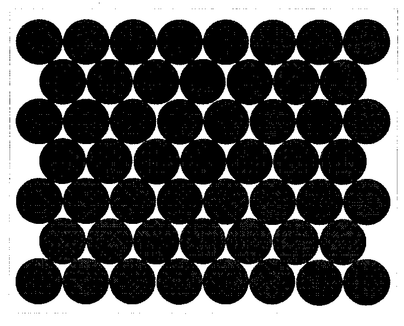
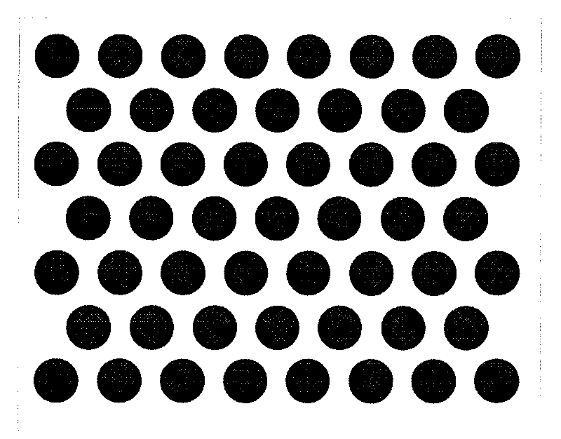
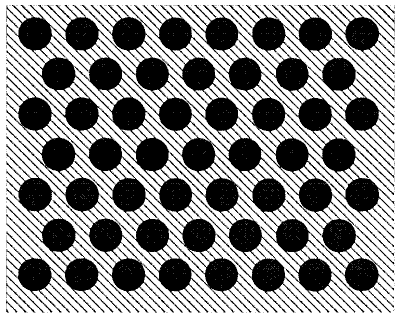
Image

Examples
Embodiment 1
[0044] Utilize the preparation method of the present invention to make the gold nano-prism structure array (square prism) that size is less than 100nm, it specifically comprises the following steps:
[0045] 1. Preparation of monolayer ordered silica nanospheres densely arranged
[0046] 1.1 Prepare the silicon wafer: first select a (110) crystal-oriented silicon wafer with a size of 25 mm × 25 mm × 0.5 mm as the substrate, and put the silicon wafer into acetone, ethanol, and deionized water for ultrasonic cleaning for 30 minutes, and then put hydrogen peroxide and 98 % concentrated sulfuric acid solution was heated to 80°C, and the ultrasonically cleaned silicon chip was soaked in it for 1 hour. Soak in the washing solution at ℃ for 1 hour, take it out and rinse it repeatedly to obtain a clean and hydrophilic surface of the silicon wafer, and place it in absolute ethanol for later use;
[0047] 1.2 Prepare the silica nanosphere sol system: take silica nanospheres with an ave...
Embodiment 2
[0061] Utilizing the preparation method of the present invention to make a copper nano cylinder array with a diameter of 120nm to 180nm and a height of 80nm, it specifically includes the following steps:
[0062] 1. Preparation of monolayer ordered silica nanospheres densely arranged
[0063] 1.1 Prepare the silicon wafer: first select a (100) crystal-oriented silicon wafer with a size of 25mm×25mm×0.5mm as the substrate, and put the silicon wafer into acetone, ethanol, and deionized water for ultrasonic cleaning for 30 minutes, and then put hydrogen peroxide and 98 % concentrated sulfuric acid solution was heated to 80°C, and the ultrasonically cleaned silicon chip was soaked in it for 1 hour. Soak in the washing solution at ℃ for 1 hour, take it out and rinse it repeatedly to obtain a clean and hydrophilic surface of the silicon wafer, and place it in absolute ethanol for later use;
[0064] 1.2 Prepare the silica nanosphere sol system: take silica nanospheres with an avera...
Embodiment 3
[0077] Utilize the preparation method of the present invention to make the aluminum nano cap structure array that diameter is about 300nm, height is about 100nm, it specifically comprises the following steps:
[0078] 1. Preparation of monolayer ordered silica nanospheres densely arranged
[0079] 1.1 Prepare the silicon wafer: first select a (100) crystal-oriented silicon wafer with a size of 25mm×25mm×0.5mm as the substrate, and put the silicon wafer into acetone, ethanol, and deionized water for ultrasonic cleaning for 30 minutes, and then put hydrogen peroxide and 98 % concentrated sulfuric acid solution was heated to 80°C, and the ultrasonically cleaned silicon chip was soaked in it for 1 hour. Soak in the washing solution at ℃ for 1 hour, take it out and rinse it repeatedly to obtain a clean and hydrophilic surface of the silicon wafer, and place it in absolute ethanol for later use;
[0080] 1.2 Prepare the silica nanosphere sol system: take silica nanospheres with an ...
PUM
| Property | Measurement | Unit |
|---|---|---|
| particle size | aaaaa | aaaaa |
| diameter | aaaaa | aaaaa |
| height | aaaaa | aaaaa |
Abstract
Description
Claims
Application Information