Packaging substrate structure for LED and production method thereof

A technology for packaging substrates and manufacturing methods, which is applied in the manufacturing of semiconductor/solid-state devices, electrical components, and electrical solid-state devices, etc., can solve problems such as the large influence of LED chips, the influence of chip luminescence, and limited application occasions, so as to improve light output and light Color distribution, improve light output efficiency and life, improve the effect of work reliability

Inactive Publication Date: 2010-06-23
SUN YAT SEN UNIV
View PDF0 Cites 12 Cited by
  • Summary
  • Abstract
  • Description
  • Claims
  • Application Information

AI Technical Summary

Problems solved by technology

The ceramic substrate has excellent performance, which is of great benefit to the reliability and life of the LED, but its disadvantages are that it is expensive, the manufacturing process is not as simple as that of the metal substrate, and the thermal conductivity is not superior enough.
[0006] Most of the existing packaging methods of LED chips adopt planar packaging, that is, the LED chips are on the same plane on the packaging substrate, so that the side light output of the LED chip is greatly affected by the packaging substrate, especially the board-integrated packaging of multi-chip LEDs. Due to the high density and small chip spacing, not only the thermal field generated by the LED chip interacts with each other, but also the side luminescence of the chip and the chip interacts with each other, and the side luminescence of the chip is affected by the packaging substrate.
Moreover, most of the features of LED planar packaging are reflective cups, which makes the light output of the packaged LEDs affected by the reflective cups, and the output angle that can be achieved is small, which may limit the application of LEDs.
[0007] And currently used in high-power integrated LED packaging substrates, due to the influence of the phosphor layer, less consideration has been given to the influence of the substrate on the light output and light color distribution of high-power white LEDs
The light distribution of the product is difficult to be uniform, the color distribution is difficult to achieve consistency in space, and the macula is still difficult to overcome

Method used


Image

  • Packaging substrate structure for LED and production method thereof
  • Packaging substrate structure for LED and production method thereof
  • Packaging substrate structure for LED and production method thereof

Examples


Embodiment 1

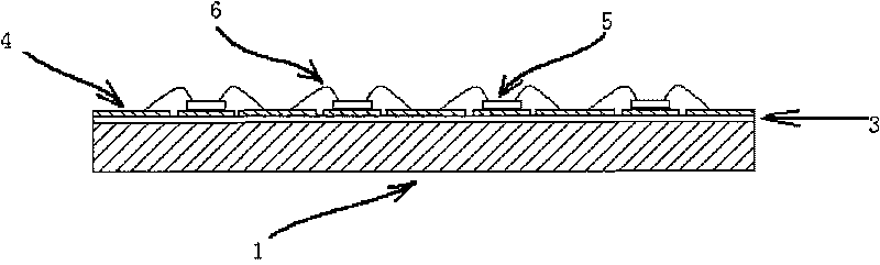
[0034] Embodiment 1: as figure 2 As shown, the substrate and the boss are made of metal materials, and the substrate outside the boss is stacked with an insulating layer 3 and a circuit connection layer 4 of a copper-clad circuit from bottom to top.

[0035]The production method is as follows: when making the metal base plate of the boss, the boss is first formed on the metal plate by stamping, rolling, melting or etching, etc., and according to the size, shape and height of the boss, the designed and manufactured The insulating layer 3 with holes and the circuit connection layer 4 are successively stacked on the metal plate, exposing the boss above the circuit connection layer. The packaged LED chip 5 is bonded on the boss by silver glue bonding or eutectic welding, and then the LED chip 5 is connected to the circuit connection layer 4 by welding gold wire 6 .

Embodiment 2

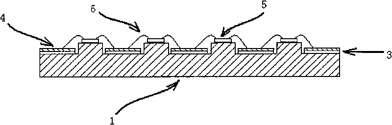
[0036] Embodiment 2: as image 3 Shown is a schematic structural diagram of a ceramic substrate with a boss structure. The substrate and the boss are made of ceramic material, and the circuit connection layer 4 formed by vapor deposition is arranged on the substrate outside the boss.

[0037] The manufacturing method is as follows: for using ceramics as the base plate, by adopting methods such as injection molding, during the sintering process of the ceramics, the bosses with specific size, shape and height are directly formed on the ceramic base plate. Then, the designed circuit connection layer 4 is vapor-deposited on the ceramic substrate. The packaged LED chip is also crystal-bonded or eutectic on the boss of the ceramic substrate, and is electrically connected to the circuit connection layer 4 through the gold wire 6 .

Embodiment 3

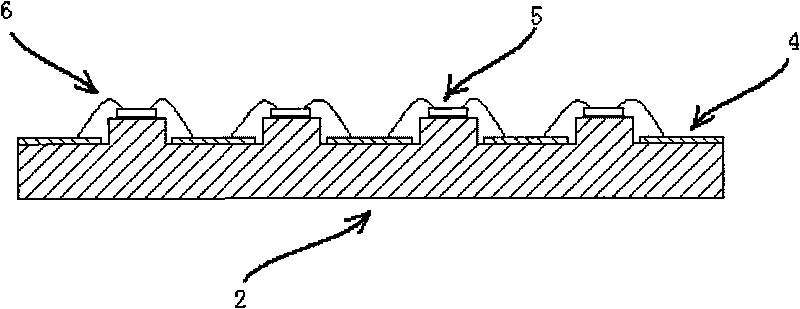
[0038] Embodiment 3: as Figure 4 , 5 As shown, for metal-ceramic hybrid substrates, the difference from the structure of Example 2 is that a hole with a certain size, shape and depth is provided at the position corresponding to the bottom surface of the substrate and the boss, and metal is melted in the hole. Or be filled with silver paste 7 . Furthermore, a metal layer of a certain thickness may be provided on the bottom of the substrate, and the metal layer is connected to the metal melted in the hole or the silver paste injected.

[0039] The production method is as follows: same as in Example 2, also in the process of ceramic sintering, a boss of a specific size is generated on the top surface of the ceramic substrate. The difference is that at the same time, at the position corresponding to the boss on the bottom of the ceramic substrate, Holes of a certain size, shape and depth are left. Then reverse the ceramic substrate, and then melt metal, such as copper, aluminu...


PUM


Abstract

The invention discloses a packaging substrate structure for an LED and a production method thereof. An LED substrate of the invention is characterized in that a boss with the specific size, shape and height is formed on a die bonding or eutectic position of a common LED substrate; and the boss is directly connected with the substrate. The substrate outside the boss is paved with a circuit connection layer. An LED chip is bonded on the boss in a die bonding or eutectic mode. Compared with the common metal PCB, the LED substrate on the boss position reduces an insulating material layer with bad heat-conducting property so that the heat generated by the high-power LED chip can be better dissipated through the substrate from the bottom. The boss structure increases the utilization of the emitted light on the lateral surface of the LED chip, improves the light-extraction efficiency, reduces the influence of the reflector cup, increases the light emergent angle, and greatly improves the light color distribution of the LED.

Description

technical field [0001] The invention relates to the field of packaging substrates for LEDs. Background technique [0002] LED is a semiconductor light-emitting device that can directly convert electrical energy into visible light and radiant energy. It has a series of characteristics such as low operating voltage, low power consumption, high luminous efficiency, light weight, and small size. Applied to indicator lights, display screens, etc. White LEDs are gradually entering the field of general lighting and are known as the fourth generation of lighting sources. With the rapid development of high-power LEDs, the luminous efficiency of LEDs is improving step by step, and the integration level of LED chips is getting higher and higher, but the heat generation per unit area is also rising. If the heat generated is not well dissipated If it goes out, it will seriously affect the reliability, efficiency and working life of the LED. Moreover, after the LED is packaged and mold...

Claims


Application Information

Patent Timeline
Patent Type & Authority Applications(China)
IPC IPC(8): H01L25/00H01L23/13H01L23/48H01L23/367H01L23/14H01L21/48
CPCH01L2224/45144H01L2224/48091
Inventor 吴昊张佰君王力蚁泽纯凌敏捷
Owner SUN YAT SEN UNIV
Why Eureka
Try Eureka