Non-refrigerant thermopile infrared detector and manufacturing method thereof

A technology for infrared detectors and manufacturing methods, applied in electric radiation detectors, piezoelectric/electrostrictive/magnetostrictive devices, piezoelectric effect/electrostrictive or magnetostrictive motors, etc., can solve problems that cannot be monitored , low device test efficiency, and the inability to reduce device costs, etc., to achieve the effects of reducing test costs, simplifying test steps, and improving test efficiency

Active Publication Date: 2010-07-14
SHANGHAI INST OF MICROSYSTEM & INFORMATION TECH CHINESE ACAD OF SCI
View PDF0 Cites 37 Cited by
  • Summary
  • Abstract
  • Description
  • Claims
  • Application Information

AI Technical Summary

Problems solved by technology

[0011] The disadvantage of the traditional thermopile infrared detector is that the vacuum degree of the detector package cannot be measured after the wafer-level vacuum packaging of the thermopile infrared detector, and the key process step of the wafer-level vacuum bonding package cannot be measured. Monitoring; aft

Method used


Image

  • Non-refrigerant thermopile infrared detector and manufacturing method thereof
  • Non-refrigerant thermopile infrared detector and manufacturing method thereof
  • Non-refrigerant thermopile infrared detector and manufacturing method thereof

Examples


Embodiment 1

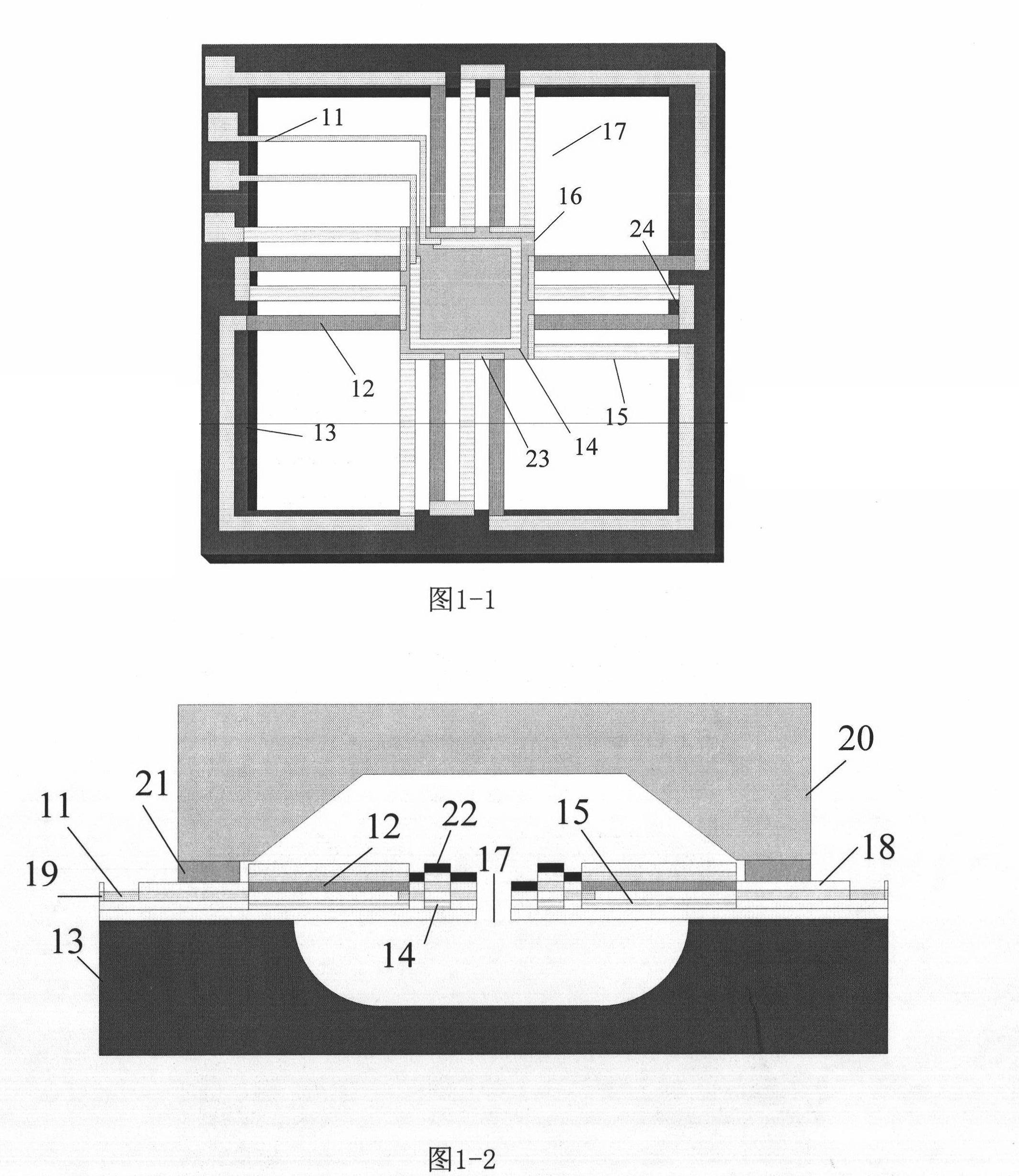
[0055] The material of the thermocouple is polysilicon and aluminum, and the material of the micro heater is polysilicon.

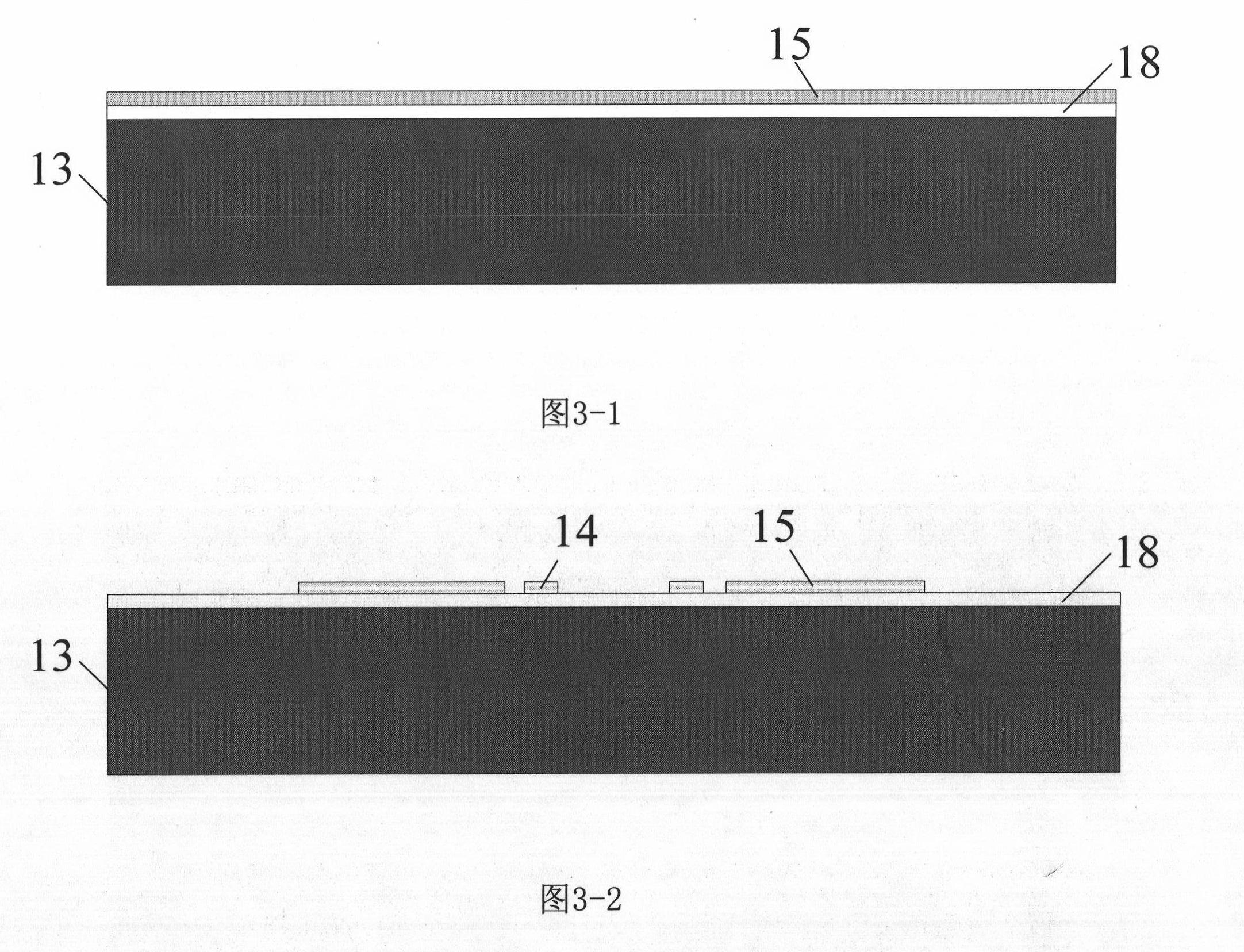
[0056] (1) Thermally grow silicon oxide 18 on the front side of the polished silicon wafer 13, and then deposit a layer of polysilicon 15 on the silicon oxide film by LPCVD. See Figure 3-1 .

[0057] (2) Doping the polysilicon film to make it conductive. Photolithographic patterning, etching to form polysilicon strips, the polysilicon 15 in the thermocouple area is used as a component of the thermocouple, and the polysilicon in the absorption area is used as a component 14 of the micro heater. See Figure 3-2 .

[0058] (3) A layer of silicon oxide 18 is deposited as an insulating layer by LPCVD or PECVD. Photoetching the lead hole pattern to remove the silicon oxide in the lead hole area. See Figure 3-3 .

[0059] (4) Deposit a layer of metal thin film aluminum by evaporation or sputtering. Photoetching metal lines, corroding metal, part of th...

Embodiment 2

[0067] The material of the thermocouple is polysilicon and aluminum, and the material of the heater is metal film.

[0068] (1) Thermally grow silicon oxide 18 on the front side of the polished silicon wafer 13, and then deposit a layer of polysilicon 15 on the silicon oxide film by LPCVD.

[0069] (2) Doping the polysilicon film to make it conductive. Photolithographic patterning, etching to form polysilicon strips, and polysilicon 15 in the thermocouple area as a component of the thermocouple.

[0070] (3) A layer of silicon oxide 18 is deposited as an insulating layer by LPCVD or PECVD. Photoetching the lead hole pattern to remove the silicon oxide in the lead hole area.

[0071] (4) Deposit a layer of metal thin film by evaporator or sputtering device. Photoetching metal lines, corroding metal, part of the metal lines 12 and the polysilicon lines in step 2 form a thermocouple pair structure, part of the metal lines 11 are used as metal wiring to realize the electrical c...

Embodiment 3

[0079] The specific implementation steps are the same as in Example 1, the main difference is: first, the polysilicon strips at the thermocouples in Step 2 of Example 1 are changed from being parallel to each side of the absorption region to being arranged at equal intervals along the radial direction of the absorption region. Second, the polysilicon heaters at the absorption region in Step 2 of Example 1 are changed to a circular arrangement, and the rest remain unchanged. The device geometry is as Figure 5 shown.


PUM


Abstract

The invention relates to a non-refrigerant thermopile infrared detector and a manufacturing method thereof. The invention is characterized in that a micro heater is arranged in the infrared absorption area of a non-refrigerant thermopile infrared detector. Because the manufacturing process of the micro heater is completely compatible with that of the thermopile, the two processes are integrated on one chip. By using the micro heater to measure the thermal conduction of the encapsulated infrared detector, the invention realizes the measurement of the vacuum degree of an encapsulated device; and by using the micro heater to simulate the operation state of the thermopile infrared detector, the invention realizes the wafer level self-test of the infrared performance of the detector. The invention can be used for mass production, can monitor the key process step of wafer level bonding and vacuum encapsulation, and can realize the wafer level measurement of the infrared performance of the detector. Besides, the invention improves the device-testing efficiency, reduces the testing cost, and can realize a low-cost and high-performance non-refrigerant thermopile infrared detector.

Description

technical field [0001] The invention relates to an uncooled thermopile infrared detector and a manufacturing method thereof, belonging to the technical field of uncooled infrared detection and microprocessing. Background technique [0002] With the increasing status of infrared detection technology in the military and civilian fields, the application range of infrared detectors is also increasing. According to the working mechanism, infrared detectors can be divided into thermal detectors and photon detectors (C G Mattsson, K.B., G H-E Nilsson and H Martin, Thermal simulation and design optimization of a thermopile infrared detector with SU-8 membrane. Journal of Micromechanics and Microengineering, 2009.19(5): p.055016.). Among them, thermal detectors are mainly divided into three types: thermocouple / thermopile, thermistors (Bolometers) and pyroelectric detectors (Pyroelectric); photon detectors are mainly divided into intrinsic type (Intrinsic), non- There are several k...

Claims


Application Information

Patent Timeline
IPC IPC(8): G01J5/12B81B7/02B81C1/00B81C3/00
Inventor 熊斌徐德辉王跃林
Owner SHANGHAI INST OF MICROSYSTEM & INFORMATION TECH CHINESE ACAD OF SCI
Why Eureka
Try Eureka