CMOS (Complementary Metal-Oxide-Semiconductor Transistor)-process compatible grid-control p-n junction forward-direction injection type silicon light-emitting device and production method thereof

A technology for light-emitting devices and manufacturing methods, which are applied in semiconductor/solid-state device manufacturing, electric solid-state devices, semiconductor devices, etc., can solve the problems of common power supply, low luminous efficiency, and inability to control light intensity, and achieve low operating voltage, high The effect of luminous intensity

Inactive Publication Date: 2012-09-05
TIANJIN POLYTECHNIC UNIV
View PDF0 Cites 0 Cited by
  • Summary
  • Abstract
  • Description
  • Claims
  • Application Information

AI Technical Summary

Problems solved by technology

However, no breakthrough has been made in the research of silicon-based light-emitting devices: p-n junction reverse avalanche breakdown type silicon-based light-emitting devices [5] Not only the luminous efficiency is low, but also the operating voltage is above 8V, so it cannot share power with CMOS technology; p-n junction forward injection silicon-based light-emitting tube [6] Although the working voltage is low, it can share power with CMOS technology, but its light intensity cannot be adjusted

Method used


Image

  • CMOS (Complementary Metal-Oxide-Semiconductor Transistor)-process compatible grid-control p-n junction forward-direction injection type silicon light-emitting device and production method thereof
  • CMOS (Complementary Metal-Oxide-Semiconductor Transistor)-process compatible grid-control p-n junction forward-direction injection type silicon light-emitting device and production method thereof
  • CMOS (Complementary Metal-Oxide-Semiconductor Transistor)-process compatible grid-control p-n junction forward-direction injection type silicon light-emitting device and production method thereof

Examples


Embodiment Construction

[0054] The present invention will be described in detail below in conjunction with the accompanying drawings and embodiments.

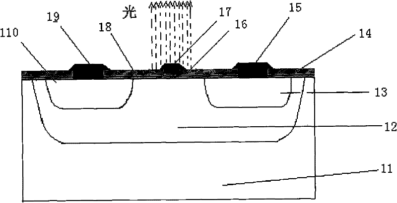
[0055] 1. Device structure and fabrication process

[0056] figure 1 A schematic diagram of the unit structure of a silicon light-emitting device in an N-well process on a P-type silicon substrate is given, and the emitter P is manufactured in the N-well 12 by ion implantation or diffusion according to a typical CMOS process flow + The doped region 110 and the N well electrically contact the N + Doping region 13, the body concentration is 8×10 18 cm -3 above. The P+ doped region 110 is completed simultaneously with the source and drain of the P-channel MOSFET; N + The doped region 13 is completed simultaneously with the source and drain of the N channel. Then, an ultra-thin gate oxide layer 18 with a thickness in the range of 3-7 nm is grown on the upper surface of the N well 12 by a thermal oxidation method (prepared simultaneously with the CMO...


PUM


Abstract

The invention belongs to the field of silicon-substrate photoelectronic technology based on micro electronic technique and relates to a CMOS (Complementary Metal-Oxide-Semiconductor Transistor)-process compatible grid-control p-n junction forward-direction injection type silicon light-emitting device and a production method thereof. The device comprises a p silicon substrate and an n well; an emitting electrode p+ doped area and an N well electrical contact N + doped area are made in the n well; an ultrathin gate oxide layer is grown on the surface of the N well; a field oxide layer and a polysilicon gate are arranged on the ultrathin gate oxide layer; an anode and a cathode are respectively made on the emitting electrode p+ doped area and the N well electrical contact N+ doped area; and a gate electrode is made on the polysilicon gate. The invention belongs to p-n junction forward-direction minority carrier injection type light-emitting devices, has low working voltage and can share one power supply with CMOS technology.

Description

technical field [0001] The invention belongs to the technical field of silicon-based optoelectronics based on microelectronic technology, and relates to a silicon light-emitting device. Background technique [0002] In recent years, under the circumstance that the feature size of CMOS devices tends to various limit values, the research and development of silicon-based optoelectronic devices has attracted increasing attention and attention from the information technology community. This is not only due to the urgent need for optical interconnection in the near future, but also the requirements for the comprehensive combination and integration of the two major information technologies of microelectronics and optoelectronics in the silicon-based monolithic integration in the future. Current silicon-based Raman lasers compatible with CMOS processes [1] , High Speed ​​Optical Modulator [2] , micro ring light modulator [3] and microring photobistability [4] And so on have been...

Claims


Application Information

Patent Timeline
Patent Type & Authority Patents(China)
IPC IPC(8): H01L27/15H01L21/8249
Inventor 郭维廉牛萍娟李晓云
Owner TIANJIN POLYTECHNIC UNIV
Why Eureka
Try Eureka