Method for preparing thin film solar cell adsorbing layer CuInSe2 film

A technology of solar cells and absorbing layers, which is applied in the manufacture of circuits, electrical components, and final products. It can solve the problems of high price of radio frequency power supply, problems of personal protection, and unsuitability for industrial production applications, and achieve raw materials saving, low cost, and easy operation. simple effect

Inactive Publication Date: 2010-07-14
SHENZHEN UNIV
View PDF0 Cites 9 Cited by
  • Summary
  • Abstract
  • Description
  • Claims
  • Application Information

AI Technical Summary

Problems solved by technology

[0005] Not long ago, Müller et al. reported in "Thin Solid film" 2006, Volume 496, page 364, that CIS films were directly prepared by radio frequency sputtering. This method omits the selenization process, but the high-power radio frequency power supply is not only expensive, but also It is also a problem for personal protection, not suitable for industrial production applications

Method used


Image

  • Method for preparing thin film solar cell adsorbing layer CuInSe2 film
  • Method for preparing thin film solar cell adsorbing layer CuInSe2 film
  • Method for preparing thin film solar cell adsorbing layer CuInSe2 film

Examples


preparation example Construction

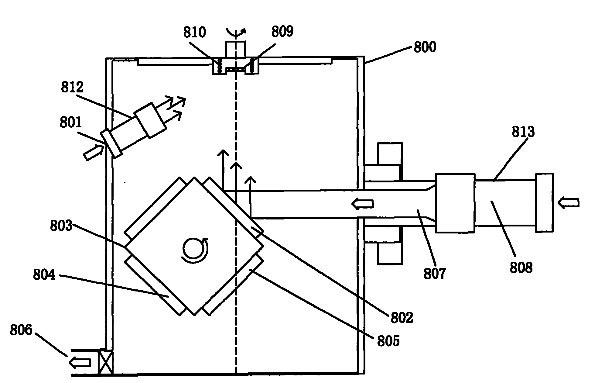
[0028] The invention provides a thin film solar cell absorption layer CuInSe 2 The preparation method of thin film, the preparation of its CIS absorption layer thin film adopts ultra-high vacuum ion beam sputtering system, such as figure 1 As shown, the ion beam sputtering system includes a vacuum chamber 800, a first high-purity argon (Ar) gas inlet 801, a Cu (copper) target position 802, a multi-station rotary frame 803, and a Se (selenium) target 804 , In (indium) target 805, vacuum extraction port 806, high-energy sputtering ion beam 807, glow discharge area 808, substrate holder 809, substrate heating seat 810, second high-purity argon (Ar) gas inlet 811, An auxiliary ion source emitting gun 812 and a main ion source emitting gun 813 .

[0029] Based on the above-mentioned ion beam sputtering system, the preparation method of the copper indium selenide film of the thin film solar cell absorption layer of the present invention, such as Figure 5 As shown, the specific st...

Embodiment 1

[0039] Example 1, BK7 optical glass is used as the substrate, and organic solvent is used for ultrasonic cleaning. A Cu target 802, an In target 805 and a Se target 804 with a purity of 99.9% are respectively mounted on a four-station rotary frame 803 to be sputtered, as figure 1 As shown, the background vacuum degree of deposition preparation is 4.0×10 -4 Pa, the working vacuum is 6.0×10 -2 Pa. Firstly, the substrate installed on the substrate holder 809 is bombarded with the Ar ion beam emitted by the auxiliary ion source emitting gun 812 for further cleaning for 5 minutes, and then the target is pre-sputtered for 20 minutes under the Ar atmosphere. Use the high-energy ion beam emitted by the main ion source gun 813 to sputter the Cu target 802 for 5.5 minutes, the In target 805 for 60 minutes, and the Se target for 60 minutes to prepare a ternary stack. The substrate is heated to 400 ° C, and the vacuum chamber 800 is vacuum Draw to 9.0×10 -4 After Pa annealing for 1h, ...

Embodiment 2

[0048] The deposition process and sputtering parameters of the thin film are the same as those in Example 1, wherein the Cu / In / Se ternary stack is changed to Cu / In / Se / Cu / In / Se ternary two-period stack, and the resulting structure and photoelectric performance are similar. For the best CIS crystal, the thickness of the film is about 1.2 μm.


PUM

PropertyMeasurementUnit
band gapaaaaaaaaaa

Abstract

The invention discloses a method for preparing a thin film solar cell adsorbing layer CuInSe2 film, comprising the following steps of: sputtering Cu, In and Se targets successively to prepare a ternary laminate or a ternary period laminate film by accurately regulating the iron beam sputtering parameter, and the like by adopting an iron beam sputtering sedimentation method, and annealing at high temperature to prepare the CuInSe2 film under the same high-vacuum environment. The method for preparing thin film solar cell adsorbing layer CuInSe2 film has optimized process and simple operation and improves the use ratio of materials; the prepared CuInSe2 film has typical copper phrite structure; the Cu/In/Se atomic ratio approaches the ideal stoichiometric ratio 1:1:2 of CIS; Cu is slightly richer than In; the optical band gap is 1.05eV; the absorption coefficient of light is as high as 105cm<-1>; and the resistivity of the thin film is less than 0.01omega cm. The invention satisfies the performance requirement of high-efficiency photovoltaic device.

Description

technical field [0001] The invention relates to the field of photoelectric functional materials, in particular to a copper indium selenide (CuInSe) absorbing layer of a thin film solar cell 2 ) film preparation method. Background technique [0002] Copper indium selenide thin film solar cells are one of the most promising photovoltaic cell technologies. Copper indium selenide (CuInSe) with a chalcopyrite structure 2 ) (referred to as CIS) is a direct bandgap I-III-VI group ternary compound semiconductor material with up to 6×10 -5 cm -1 The advantages of light absorption rate, band gap of 1.04eV and strong radiation resistance make it a better absorbing layer material in thin film solar cells. [0003] At present, the more commonly used preparation methods of CIS thin films are three-step co-evaporation method and selenization method after CuIn prefabricated layer. U.S. Renewable Energy National Laboratory (NREL) I.Repins et al. reported in the literature on page 235 of...

Claims


Application Information

Patent Timeline
Patent Type & Authority Applications(China)
IPC IPC(8): H01L31/18
CPCY02P70/50
Inventor 范平梁广兴郑壮豪张东平蔡兴民
Owner SHENZHEN UNIV
Why Eureka
Try Eureka