Method for preparing thin film solar cell adsorbing layer CuInSe2 film
A technology of solar cells and absorbing layers, which is applied in the manufacture of circuits, electrical components, and final products. It can solve the problems of unsuitability for industrial production applications, personal protection problems, and high prices of radio frequency power supplies, and achieve raw material saving, low cost, and simple operation. Effect
- Summary
- Abstract
- Description
- Claims
- Application Information
AI Technical Summary
Problems solved by technology
Method used
Image
Examples
preparation example Construction
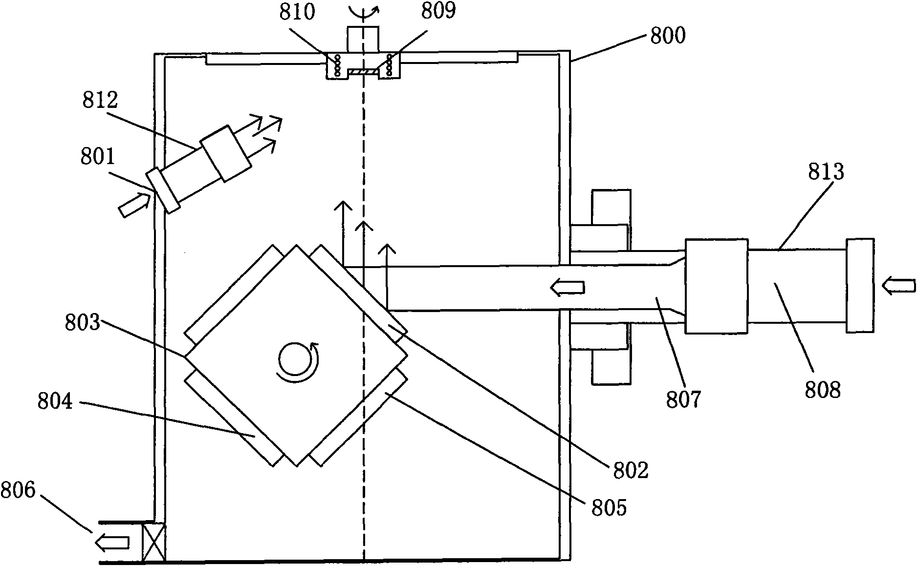
[0028] The invention provides a thin film solar cell absorption layer CuInSe 2 The preparation method of thin film, the preparation of its CIS absorption layer thin film adopts ultra-high vacuum ion beam sputtering system, such as figure 1 As shown, the ion beam sputtering system includes a vacuum chamber 800, a first high-purity argon (Ar) gas inlet 801, a Cu (copper) target position 802, a multi-station rotary frame 803, and a Se (selenium) target 804 , In (indium) target 805, vacuum extraction port 806, high-energy sputtering ion beam 807, glow discharge area 808, substrate holder 809, substrate heating seat 810, second high-purity argon (Ar) gas inlet 811, An auxiliary ion source emitting gun 812 and a main ion source emitting gun 813 .
[0029] Based on the above-mentioned ion beam sputtering system, the preparation method of the copper indium selenide film of the thin film solar cell absorption layer of the present invention, such as Figure 5 As shown, the specific st...
Embodiment 1
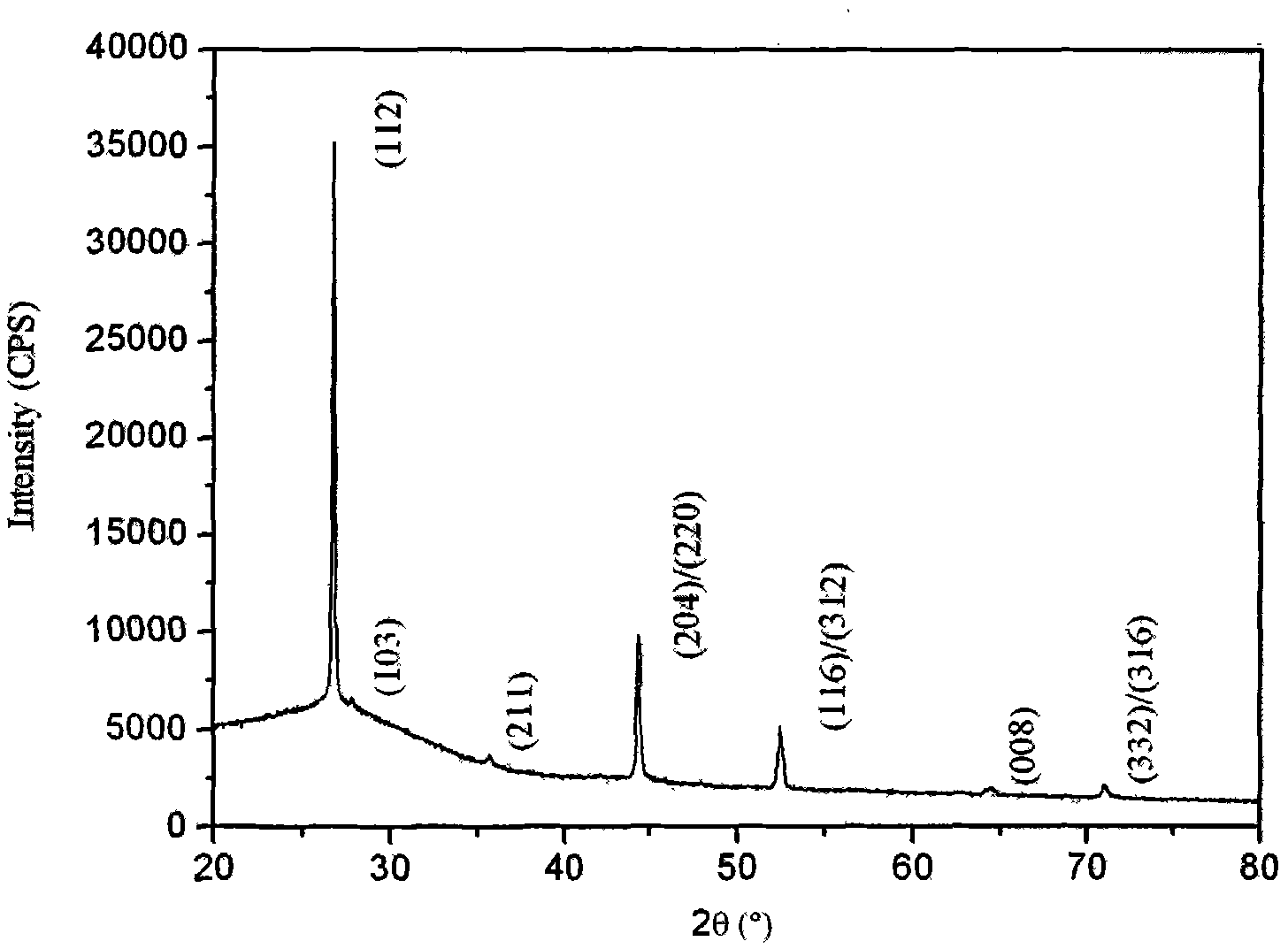
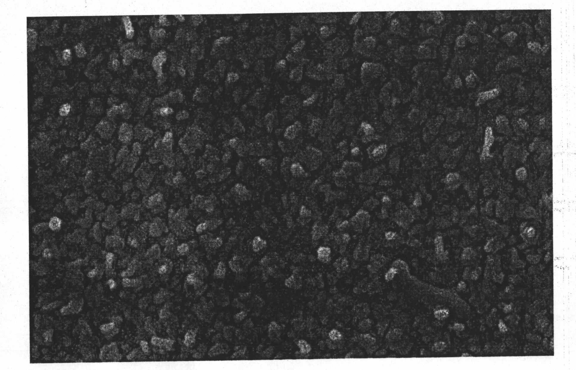
[0039] Example 1, BK7 optical glass is used as the substrate, and organic solvent is used for ultrasonic cleaning. A Cu target 802, an In target 805 and a Se target 804 with a purity of 99.9% are respectively mounted on a four-station rotary frame 803 to be sputtered, as figure 1 As shown, the background vacuum degree of deposition preparation is 4.0×10 -4 Pa, the working vacuum is 6.0×10 -2 Pa. Firstly, the substrate installed on the substrate holder 809 is bombarded with the Ar ion beam emitted by the auxiliary ion source emitting gun 812 for further cleaning for 5 minutes, and then the target is pre-sputtered for 20 minutes under the Ar atmosphere. Use the high-energy ion beam emitted by the main ion source gun 813 to sputter the Cu target 802 for 5.5 minutes, the In target 805 for 60 minutes, and the Se target for 60 minutes to prepare a ternary stack. The substrate is heated to 400 ° C, and the vacuum chamber 800 is vacuum Draw to 9.0×10 -4 After Pa annealing for 1h, ...
Embodiment 2
[0048] The deposition process and sputtering parameters of the thin film are the same as those in Example 1, wherein the Cu / In / Se ternary stack is changed to Cu / In / Se / Cu / In / Se ternary two-period stack, and the resulting structure and photoelectric performance are similar. For the best CIS crystal, the thickness of the film is about 1.2 μm.
PUM
| Property | Measurement | Unit |
|---|---|---|
| band gap | aaaaa | aaaaa |
Abstract
Description
Claims
Application Information


