

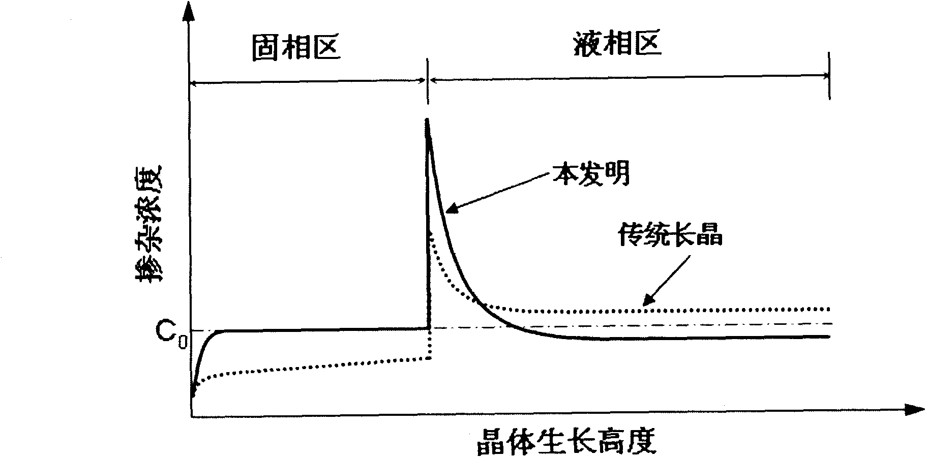
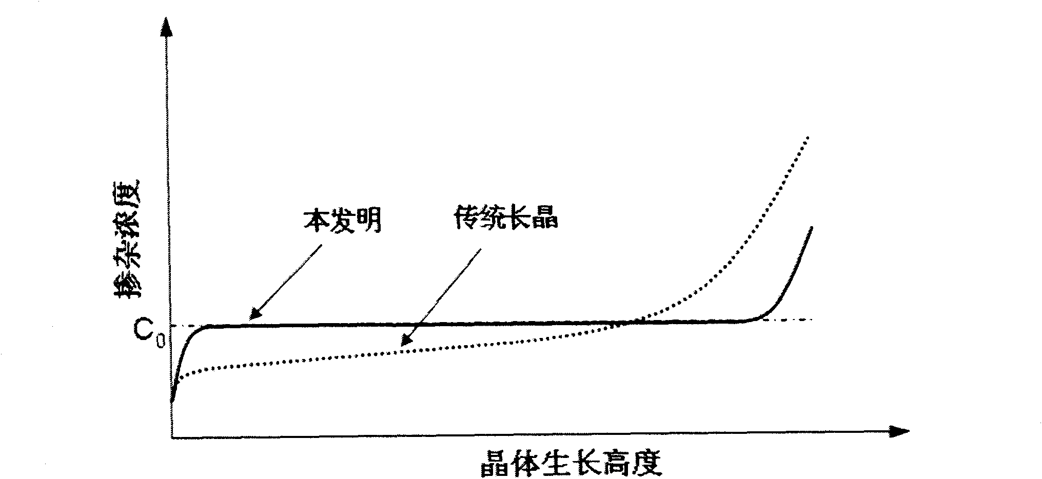
Method for preparing gallium-doped p-type crystalline silicon
A crystalline silicon, p-type technology, applied in crystal growth, chemical instruments and methods, single crystal growth, etc., can solve the problems of reducing the comprehensive electrical properties of silicon wafers, achieve cost feasibility, reduce deviation range, and increase Ga content Effect
- Summary
- Abstract
- Description
- Claims
- Application Information
AI Technical Summary
Problems solved by technology
Method used
Image

Examples
Embodiment 1
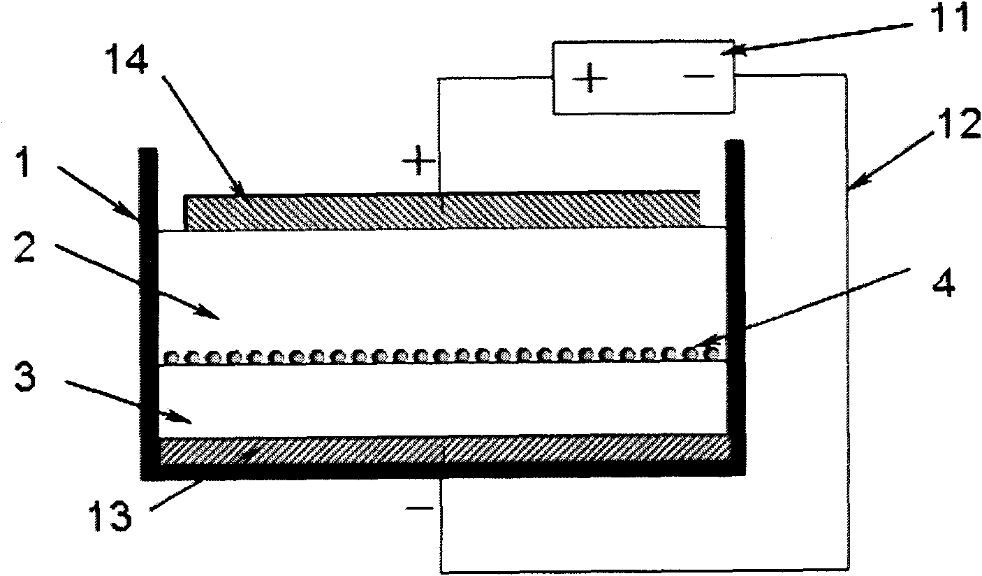
[0028] Ga-doped p-type polysilicon ingots are prepared by directional solidification under the action of a DC electric field, see Figure 3, and the following steps are adopted:
[0029] 1) Calculate the Ga doping concentration required for the corresponding silicon material according to the electrical performance requirements of the silicon wafer, and prepare the dopant.
[0030] 2) Set cathode 13 at the bottom of crucible 1, put silicon material and dopant into crucible 1 according to a certain ratio, then set anode 14 above the silicon material, connect cathode 13 to the negative pole of DC power supply 11 with wire 12, anode 14 Connect to the positive pole. When arranging the electrodes, pay attention to make the direction of the electric field parallel to the growth direction of the crystal. The anode 14 and the cathode 13 are made of high-purity graphite, and the wire 12 is made of high-purity molybdenum wire.
[0031] 3) Place the filled crucible 1 in the furnace cavity...
Embodiment 2
[0036] Ga-doped p-type single crystal silicon rods are drawn by the CZ method under the action of a DC electric field, see Figure 4, and the following steps are used to achieve:
[0037] 1) Calculate the doping concentration required for the corresponding silicon material according to the electrical performance requirements of the silicon wafer, and prepare the dopant.
[0038] 2) The crucible 1 made of high-purity graphite is used as the anode, and is connected to the positive electrode of the power supply 11 with a wire 12; silicon material and dopant are put into the crucible 1 according to a certain ratio, heated to melt the silicon material, and the temperature control system is adjusted to start Pulling, after completing the necking and shoulder growth and entering the equal-diameter growth stage, the growth crystal 3 is connected to the negative electrode of the power supply 11 as the cathode,
[0039] 3) Start to apply a DC electric field to the silicon liquid 2, the vol...
Embodiment 3
[0044] The FZ method is used to grow Ga-doped p-type single crystal silicon rods under the action of a DC electric field, see Figure 5, and the following steps are used to achieve:
[0045] 1) Calculate the doping concentration required for the corresponding silicon material according to the electrical performance requirements of the silicon wafer, and prepare the dopant. The dopant can be added in advance to the silicon rod 5 to be melted or added during the zone melting process.
[0046] 2) Assuming that the induction coil 20 moves from bottom to top, the growing crystal 3 is used as the cathode, and the crystal to be melted 5 is used as the anode, and are respectively connected to the negative pole and the positive pole of the power supply 11 by wires 12 .
[0047] 3) Increase the power of the induction coil 20 to melt the part of the silicon rod 5 to be melted, and start to apply an electric field to the silicon liquid 2. The voltage between the electrodes is 0.1-10V or the...
PUM
 Abstract
Description
Claims
Application Information