

High-transmissivity flexible transparent conductive film and preparation method thereof
A transparent conductive film, high transmittance technology, applied in conductive materials, conductive materials, cable/conductor manufacturing, etc., can solve the problems of low film transmittance and single film structure, and achieve low cost and photoelectric performance. Improved, improved light transmission efficiency
- Summary
- Abstract
- Description
- Claims
- Application Information
AI Technical Summary
Problems solved by technology
Method used
Image

Examples
Embodiment 1
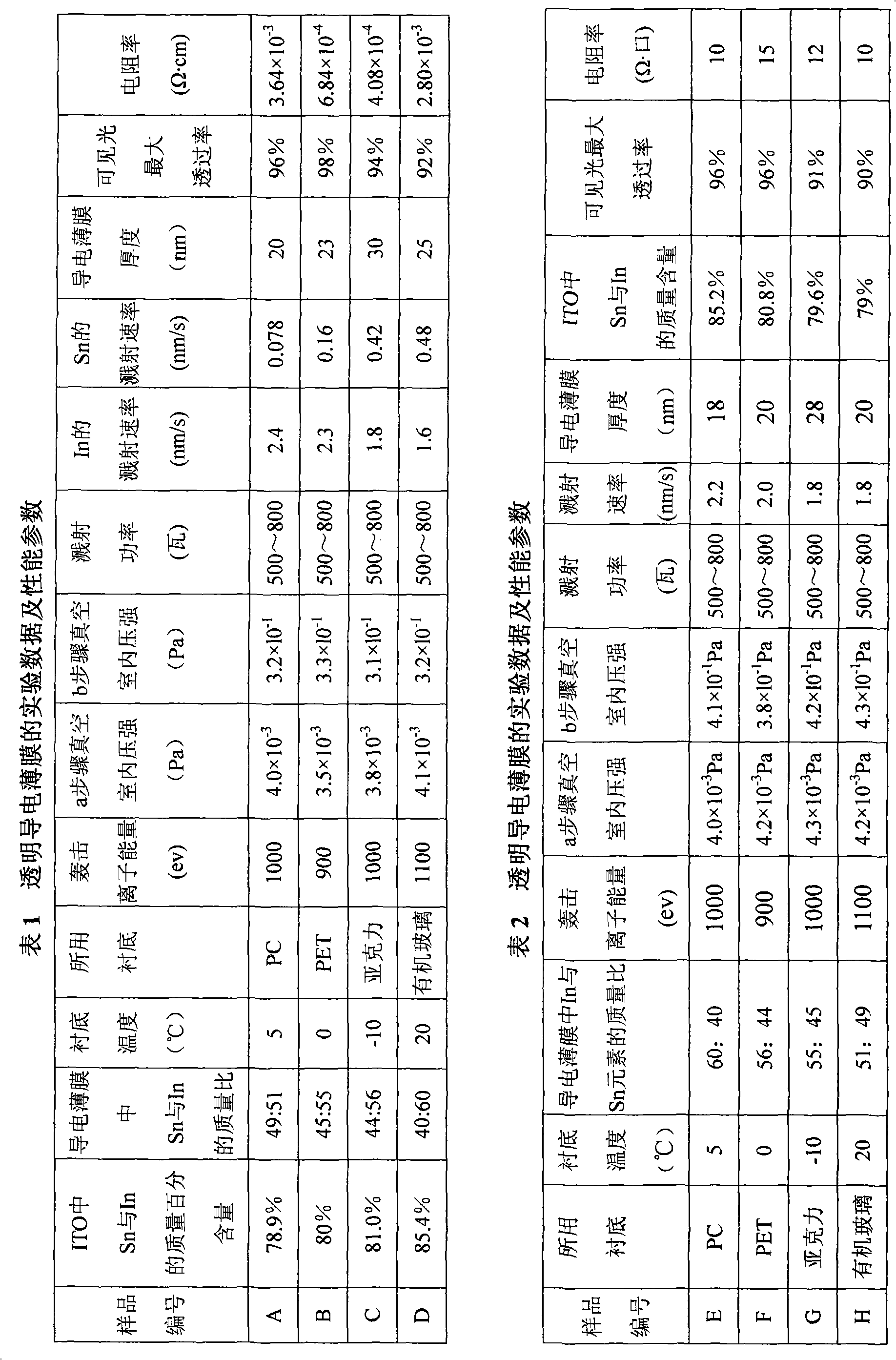
[0024] The roll-to-roll vacuum coating machine designed and manufactured by Shenyang Fushen Vacuum Equipment Co., Ltd. is used to prepare the multi-layer flexible transparent conductive film of the present invention by using DC magnetron sputtering and intermediate frequency magnetron sputtering methods. Four samples A, B, and C The specific preparation steps of D and D are as follows:
[0025] a. Put the substrate material into the vacuum chamber, and evacuate the vacuum chamber until the pressure in the chamber is lower than 5.0×10 -3 Pa, then bombard the substrate with an ion source, and the bombardment energy is >700ev;
[0026] b. Fill the vacuum chamber with oxygen and argon, the purity of the oxygen and argon in the vacuum chamber is 99.999%, after filling the oxygen and argon, control the pressure in the vacuum chamber to be 2×10 -1 Pa~5×10 -1 Within the range of Pa, the vacuum gauge and mass flow meter are used to monitor the vacuum degree of oxygen and argon filled...
Embodiment 2
[0033] Steps "a", "b" and "c" are the same as in Example 1, and step "d" is to use In with a purity of 99.99%. 2 o 3 Powder with 99.99% pure SnO 2 The powder is evenly mixed, and sintered into a target by conventional hot isostatic pressing method, and the target is used to deposit a thin film by DC magnetron sputtering technology; wherein, the substrate temperature is -10-20°C, and the sputtering power is DC 500 ~1500 watts, the sputtering rate is 0.04~3nm / s.
[0034] After the H sample is sputtered on the target, a layer of SiO is sputtered 2 , with a thickness of 1 nm.
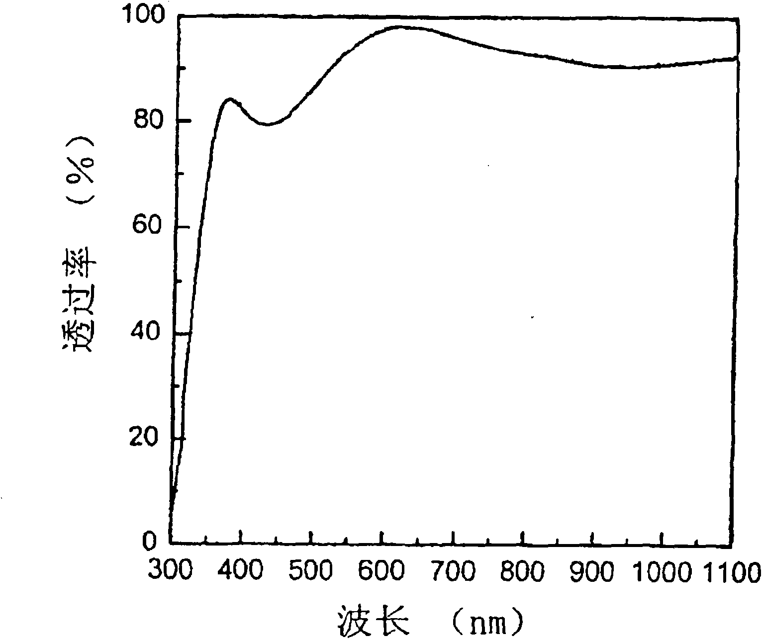
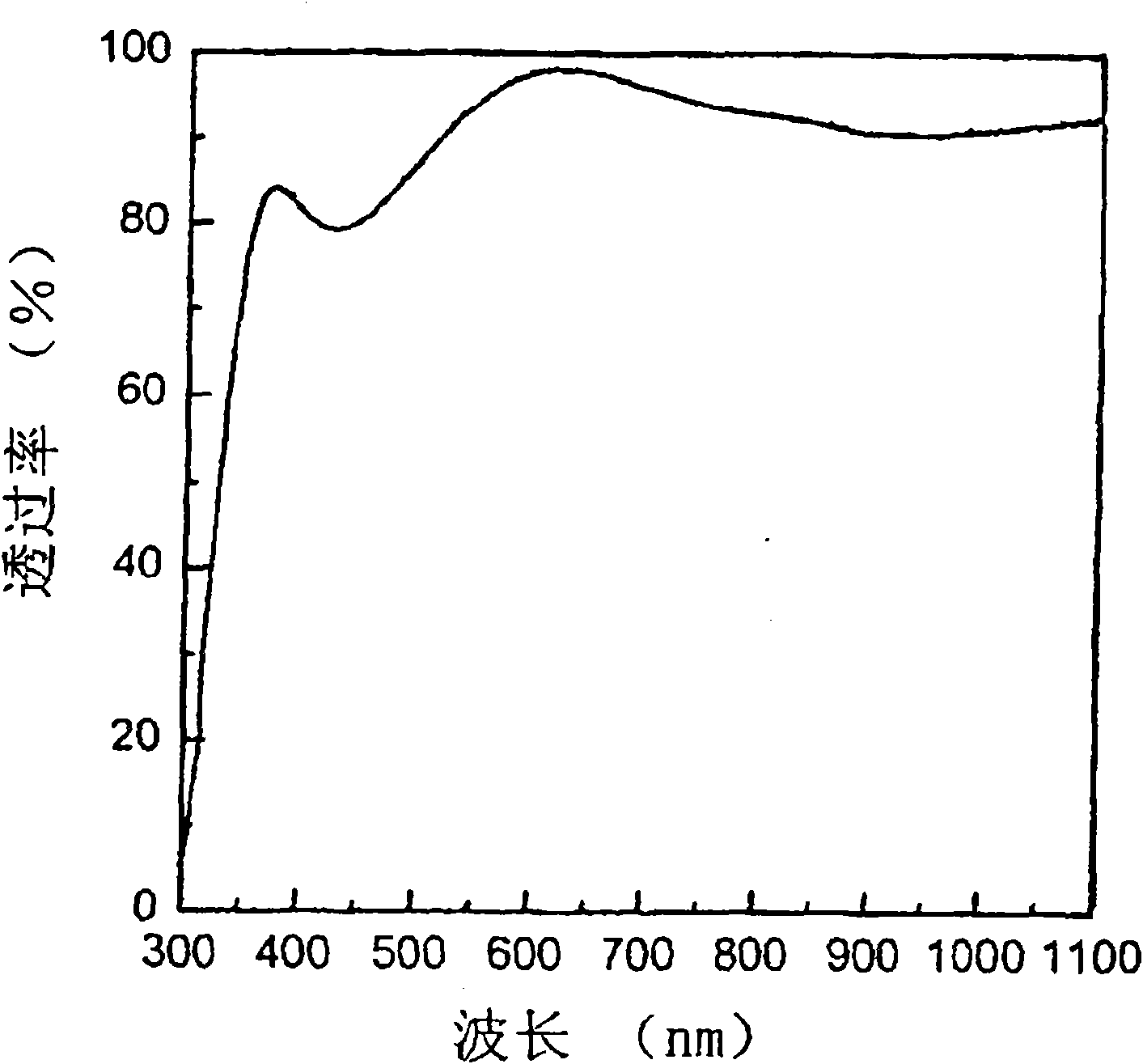
[0035] The surface resistance of the ITO thin film reaches 10-15Ω / port, and the average visible light transmittance is higher than 90%. The experimental data and the performance parameters of the prepared transparent conductive film are as shown in Table 2 for four samples E, F, G and H:
[0036]
PUM
| Property | Measurement | Unit |
|---|---|---|
| Thickness | aaaaa | aaaaa |
| Thickness | aaaaa | aaaaa |
| Thickness | aaaaa | aaaaa |
Abstract
Description
Claims
Application Information