LED large-area controllable surface coarsening and etching method based on laser

A surface roughening and laser technology, used in semiconductor devices, electrical components, circuits, etc., can solve the problems of high purchase and use costs of etching equipment, reduced electrical performance of LEDs, and difficulty in accurately controlling the rate and depth of corrosion. Low cost of equipment and use, improved current injection efficiency, and improved light extraction efficiency

Inactive Publication Date: 2010-10-20
SHANDONG UNIV
View PDF4 Cites 10 Cited by
  • Summary
  • Abstract
  • Description
  • Claims
  • Application Information

AI Technical Summary

Problems solved by technology

The disadvantages of using etching to roughen the light-emitting surface of LEDs are: (1) etching is very destructive to the carrier transport properties of semiconductor materials, which significantly reduces the electrical properties of LEDs; (2) ) The cost of purchasing and using etching equipment is extremely high, which greatly increases the cost of LEDs; (3) There is no way to control and optimize the shape and size of the roughened LED light-emitting surface by etching
(4) The processing time is longer and the production efficiency is lower
The disadvantages of using chemical corrosion to roughen the light-emitting surface of LEDs are: (1) it is difficult to accurately control the rate and depth of corrosion, which is determined by the inherent defects of chemical methods; (2) it is susceptible to external environmental temperature and other factors imp

Method used


Image

  • LED large-area controllable surface coarsening and etching method based on laser
  • LED large-area controllable surface coarsening and etching method based on laser
  • LED large-area controllable surface coarsening and etching method based on laser

Examples


Example Embodiment

[0036] Example 1:

[0037] Taking a 2-inch GaN-based front-mounted LED epitaxial wafer as an example to illustrate the implementation method of the present invention:

[0038] (1) The structure of GaN-based front-mounted LED epitaxial wafer from bottom to top is sapphire, silicon carbide or silicon substrate, buffer layer GaN, intrinsic GaN layer, n-GaN confinement layer, multiple quantum well active light-emitting region, p - GaN confinement layer.

[0039] (2) Roughening is performed on the p-GaN confinement layer, and the thickness of the p-GaN confinement layer is about 200 nm.

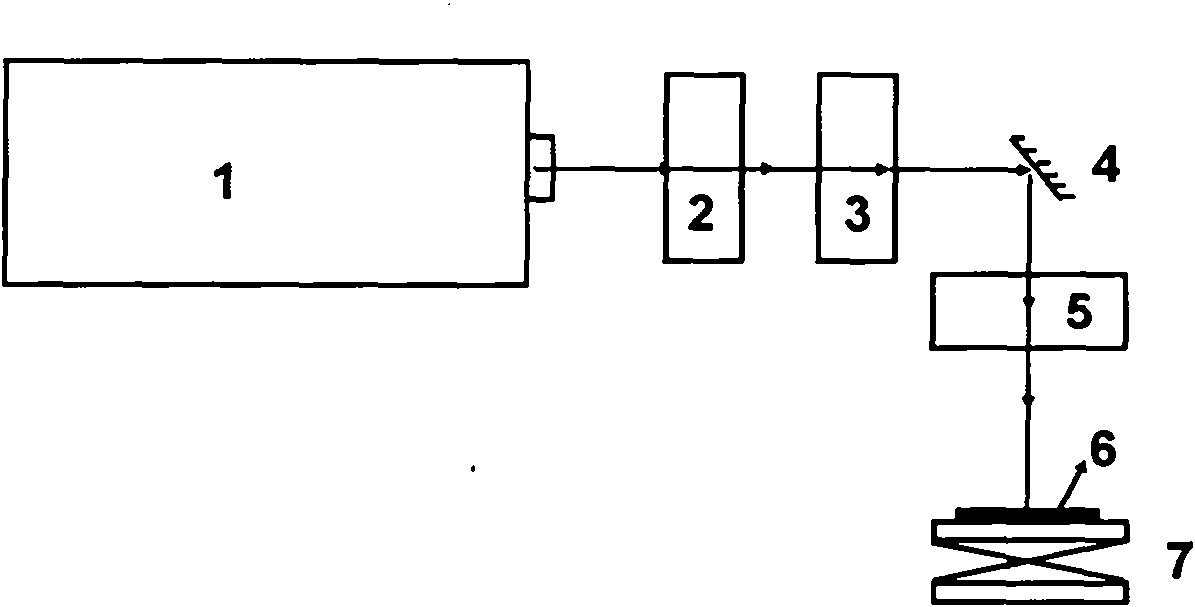
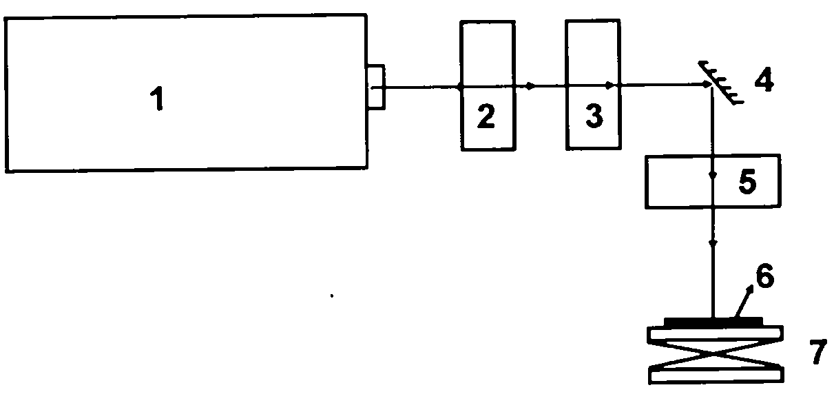
[0040] (3) Turn on the UV 355nm laser to make its laser output in a standby state.

[0041] (4) Adjust the laser beam shaping module to obtain the beam energy distribution required for processing.

[0042] (5) Fix the GaN-based front-mounted LED epitaxial wafer at the center of the elevating sample stage, adjust the elevating sample stage so that the ultraviolet 355nm laser beam is located in t...

Example Embodiment

[0048] Example 2:

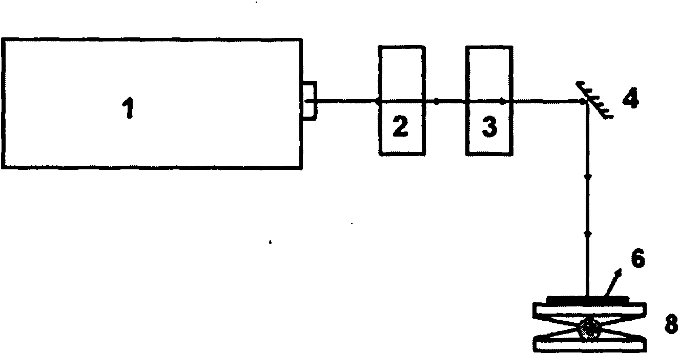
[0049] Taking a 2-inch GaN-based vertical process LED epitaxial wafer as an example to illustrate the implementation method of the present invention, the 4th, 5th, 9th, and 10th steps are the same as those in Example 1, and the differences are:

[0050] (1) The structure of the GaN-based vertical process LED epitaxial wafer from bottom to top is silicon substrate, p-GaN confinement layer, multiple quantum well active light-emitting region, n-GaN confinement layer, and intrinsic GaN.

[0051] (2) Roughening is performed on the intrinsic GaN layer, and the thickness of the intrinsic GaN layer is about 1.5 μm.

[0052] (3) Turn on the UV 355nm laser to make its laser output in a standby state.

[0053] (6) Import the required roughing processing pattern into the high-precision electric stage control software, such as a vertical, horizontal and vertical stripe structure with a period of 15 microns, a processing duty ratio of 50%, and a processing area of ​​​​c...

Example Embodiment

[0056] Example 3:

[0057] Taking a 2-inch GaAs red LED epitaxial wafer as an example to illustrate the implementation method of the present invention, the 4th, 5th, 9th, and 10th steps are the same as those in Example 1, and the differences are:

[0058] (1) The structure of GaAs red LED epitaxial wafer from bottom to top is GaAs substrate, n-GaAs confinement layer, multiple quantum well active light-emitting region, p-GaAs confinement layer, and GaP window layer.

[0059] (2) Roughening is performed on the GaP window layer, and the thickness of the GaP window layer is about 8 microns.

[0060] (3) Turn on the 532nm laser so that its laser output is in a standby state.

[0061] (6) Import the required roughing processing pattern into the high-speed galvanometer control software, such as the concentric ring structure with an inner and outer layer interval of 20 microns, the processing duty cycle is 50%, and the processing area is to cover all 2 inches of GaAs red Light LED e...


PUM

PropertyMeasurementUnit
Thicknessaaaaaaaaaa

Abstract

The invention relates to an LED large-area controllable surface coarsening and etching method based on a laser, belonging to the technical field of an LED. The method utilizes semiconductor material for carrying out strong absorption generating gasification on high-power laser with the wavelength less than the band edge absorption wavelength of the semiconductor material, thus realizing surface coarsening for the semiconductor material on the surface of the LED. A high-speed galvanometer or a precise displacement platform is used for controlling the laser processing area or pattern, and can be used for controlling the laser power and the processing line width and depth of focus level adjustment. The LED large-area controllable surface coarsening and etching method can be applied to surface coarsening and etching of the GaAs-based LED and the GaN-based LED of various structures. The laser takes the wavelength less than the band edge absorption wavelength of the processed semiconductor material as reference. The method has the advantages of wide applicable material, rapid processing speed, large area, low cost, good coarsening effect, low damage for the semiconductor material, high controllability of system processing parameters and the like, can effectively solve the problem of p-GaN layer coarsening, and has great application potential in the production of the high-brightness LED.

Description

Technical field: [0001] The invention relates to a laser-based large-area controllable surface roughening and etching method for LEDs, belonging to the technical field of light-emitting diode manufacturing. Background technique: [0002] In the 1950s, with the efforts of many well-known research institutions represented by IBM Thomas J. Watson Research Center, III-V semiconductors represented by GaAs rose rapidly in the field of semiconductor light emitting. Later, with the emergence of metal oxide chemical vapor deposition (MOCVD) technology, the growth of high-quality III-V semiconductors broke through the technical barrier, and semiconductor light-emitting diode devices with various wavelengths flooded into the market one after another. Compared with the current light-emitting devices, semiconductor light-emitting diodes have the characteristics of high theoretical efficiency, long life, and mechanical shock resistance, and are regarded as a new generation of lighting dev...

Claims


Application Information

Patent Timeline
IPC IPC(8): H01L33/00H01L33/22
Inventor 刘铎左致远张百涛何京良徐现刚
Owner SHANDONG UNIV
Why Eureka
Try Eureka