Preparation method of solar cell with buried charge layer
What is AI technical title?
AI technical title is built by Patsnap AI team. It summarizes the technical point description of the patent document.
A technology of solar cells and electric charges, applied in circuits, electrical components, and final product manufacturing, etc., can solve problems such as poor resistance to high-energy particle damage
Active Publication Date: 2010-11-10
南通东湖国际商务服务有限公司
View PDF4 Cites 29 Cited by
Summary
Abstract
Description
Claims
Application Information
AI Technical Summary
This helps you quickly interpret patents by identifying the three key elements:
Problems solved by technology
Method used
Benefits of technology
Problems solved by technology
But this P + The field is easily attenuated by the radiation of high-energy particles in space, and its ability to resist damage by high-energy particles is poor compared to BSR cells; (5) high-efficiency and low-resistance silicon solar cells (RESC), which use 0.2Ωcm and 0.3Ωcm p A battery made of molten silicon in the type area, which is characterized in that a passivation layer is prepared in the emission area of the battery
Method used
Image
Click on the blue label to locate the original text in one second.
Reading with bidirectional positioning of images and text.
Examples
Embodiment 1
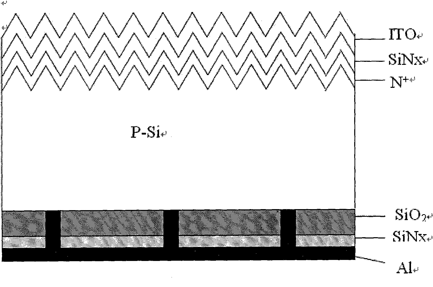
[0026] 1. The structural design of the solar cell see figure 1 .
[0027] 2. Preparation of solar cells
[0028] A (100)p-type silicon wafer is selected, with a resistivity of 3Ωcm and a thickness of 200μm.
[0030] Oxygen flow, gas flow rate 1L / min, oxidation temperature 1050°C, 20 minutes, grow a 45-50nm thick silicon oxide layer;
[0031] 2. Texturing:
[0032] Use diluted 5% HF solution to remove the oxide layer on the front surface, and use NaOH plus C 2 h 5 The OH method corrodes the texture, the temperature of the lye is about 80°C, the concentration is 1-2%, and the corrosion time is 15 minutes.
[0034] The diffusion furnace is heated up to the diffusion temperature (850-900° C.) in advance. Nitrogen gas (800ml / min) is introduced first, the silicon wafer is pushed into the constant temperature zone, and preheated for 5 minutes. Then, the nitrogen flow rate was adjusted to 60ml / min, and simultaneously the flo...
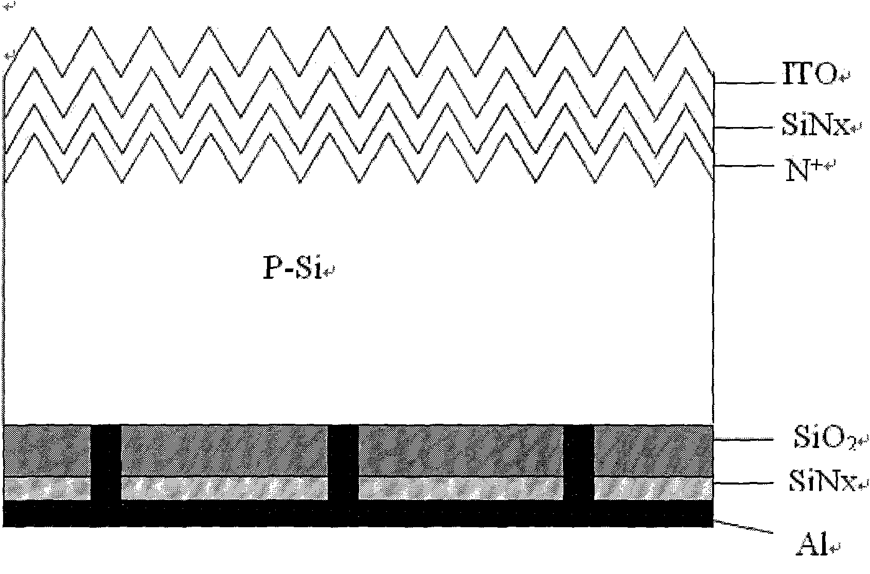
Embodiment 2
[0055] The difference between scheme two and scheme one is only in the formation process of silicon dioxide, that is, the fifth step in the specific implementation scheme. The rest of the steps are the same.
[0057] Use H 2 N(CH 2 ) 3 Si(OEt) 3 As a silicon source, water (H 2 O) and O 3 As an oxygen source, H 2 N(CH 2 ) 3 Si(OEt) 3 Pulse time is 1s, H 2 O pulse time is 400ms, O 3 The pulse time is 300ms, the cleaning gas is nitrogen, the pulse time is 2s, the substrate temperature is 100-200°C, the working pressure is 0.08-0.10Torr, the total pulse of precursor injection is 2400 times, and the cleaning pulse is 2400 times.
[0058] Implementation effect: Finally, the performance test of the battery is carried out, at AM1.5, 100mW / cm 2 Under the irradiation of standard light intensity, the open-circuit voltage of the 4.0cm×4.0cm monocrystalline silicon solar...
technical field [0001] The invention relates to a monocrystalline silicon solar cell and a preparation method thereof, in particular to a monocrystalline silicon solar cell utilizing a charge buried layer introduced into a passivation medium layer. The invention belongs to the technical field of solar cell device preparation. Background technique [0002] Energy shortage and environmental damage have made clean energy solar cells attract great attention worldwide. Many governments and civil organizations have invested a lot of manpower and financial resources in the development and production of clean energy solar cells. The low efficiency of solar cells is one of the key factors affecting its application, and it is also a difficult problem that scientists all over the world are eager to solve. The main obstacles restricting the further improvement of the photoelectric conversion efficiency of crystalline silicon solar cells are: (1) the influence of grid lines on the surfa...
Claims
Application Information
Patent Timeline
Application Date:The date an application was filed.
Publication Date:The date a patent or application was officially published.
First Publication Date:The earliest publication date of a patent with the same application number.
Issue Date:Publication date of the patent grant document.
PCT Entry Date:The Entry date of PCT National Phase.
Estimated Expiry Date:The statutory expiry date of a patent right according to the Patent Law, and it is the longest term of protection that the patent right can achieve without the termination of the patent right due to other reasons(Term extension factor has been taken into account ).
Invalid Date:Actual expiry date is based on effective date or publication date of legal transaction data of invalid patent.

