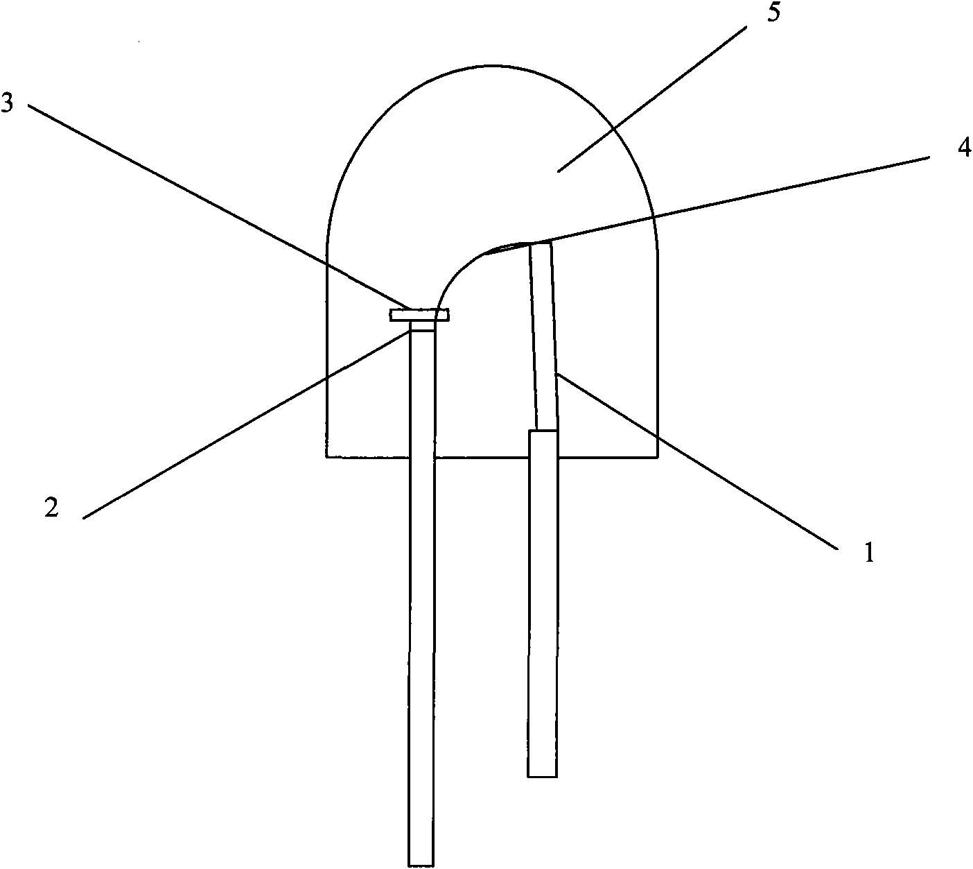
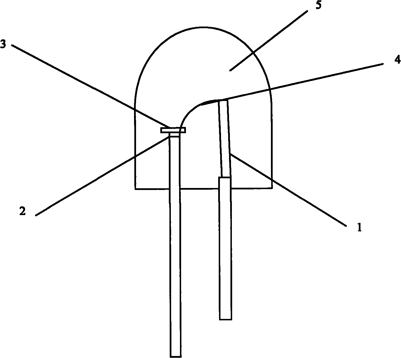
Method for manufacturing white light LED by single crystals
A manufacturing method and single crystal technology, applied in semiconductor devices, electrical components, circuits, etc., can solve the problems that white light LEDs are not involved, and achieve good physical and chemical stability, excellent thermal conductivity, and timely heat dissipation
- Summary
- Abstract
- Description
- Claims
- Application Information
AI Technical Summary
Problems solved by technology
Method used
Image
Examples
example 1
[0008] Example 1: Using 61% Al 2 o 3 , 35%Y 2 o 3 and 4% CeO 2 The proportioned raw materials are mixed and put into a 60mm diameter iridium crucible, heated to 1970°C in a D400 single crystal furnace to melt, and the pure YAG single crystal rod is used as the seed crystal for crystal growth, the rotation speed is 12r / min, and the diameter is drawn The speed is 2.0mm / h, and the size of the grown crystal is 20mm in diameter and 83mm in length. Fix the grown crystal on the glass according to the required size and cut it with a carbon cutting machine, soak the wafer in acetone for grinding and polishing, microscopically observe that there are no blisters and defects, and then polish it for more than 6 hours. The size of the chip is a single chip with a thickness of 0.2mm and a side length of 1.2mm. The single chip is packaged on an LED chip with a rated power of 1w (the size of a single LED light-emitting chip is 1mm×1mm) with a shadowless adhesive to complete the packaging o...
example 2
[0009] Example 2: Using 65% Al 2 o 3 , 33%Y 2 o 3 and 2% CeO 2 The proportioned raw materials are mixed and put into a 60mm-diameter iridium crucible, heated to 1970°C in a D400 single crystal furnace to melt, and the pure YAG single crystal rod is used as a seed crystal to grow the crystal at a speed of 12r / min. It is 2.0mm / h, and the growth crystal size is 18mm in diameter and 63mm in length. Grind and polish the wafer, observe microscopically that there are no blisters and defects, and then polish for more than 6 hours. After polishing, the single crystal is processed into a sheet with a thickness of 0.5mm and a side length of about 2.2mm, and is packaged with a shadowless adhesive. On an LED chip with a power of 3w (the size of a single LED chip is 2mm×2mm), the adjusted current is 300-750mA, which is higher than the maximum current of 650mA of the phosphor-encapsulated white LED, and the voltage is 0-3.6V. Good, the color of white light is soft and soft, the heat dis...
example 3
[0010] Example 3: Using 59% Al 2 o 3 , 40%Y 2 o 3 and 1% CeO 2 The proportioned raw materials are mixed and put into a 60mm-diameter iridium crucible, heated to 1970°C in a D400 single crystal furnace to melt, and the pure YAG single crystal rod is used as a seed crystal for crystal growth. The crystal growth rate is 2.2mm / h, and the growth crystal size is 9.5mm in diameter and 28.0mm in length; the single crystal is polished and processed into a sheet with a thickness of 0.8mm and a side length of 2.5mm, and is packaged in a 3w LED chip with a shadowless adhesive (The size of a single LED light-emitting chip is 2mm×2mm), the adjustment current is 300-750mA, which is higher than the rated current of 650mA of the phosphor-packaged white LED, and the voltage is 0-3.6V. The luminous performance is good, and the color temperature of white light is in About 6000K, the heat dissipation temperature is more than 40% lower than that of phosphor, and the luminous flux is slightly lo...
PUM
 Abstract
Description
Claims
Application Information

