
Polishing pad for chemical mechanical planarization and manufacturing method thereof

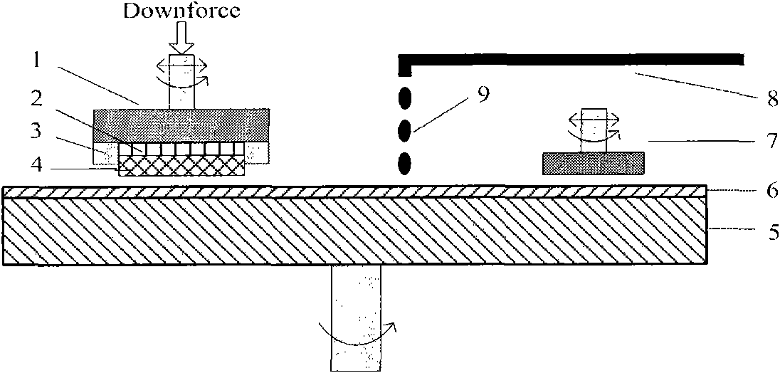
A chemical machinery, manufacturing method technology, applied in the direction of manufacturing tools, grinding/polishing equipment, wheels with flexible working parts, etc., can solve problems such as scratches, over-polishing, complexity, etc. The effect of good process controllability and simple production method

Inactive Publication Date: 2013-05-22
TSINGHUA UNIV
View PDF2 Cites 0 Cited by
  • Summary
  • Abstract
  • Description
  • Claims
  • Application Information

AI Technical Summary

Problems solved by technology

[0007] The present invention proposes a novel flexible nano-brush polishing pad for defects such as scratches, over-throwing, butterfly and erosion that may occur in the existing chemical mechanical planarization technology, especially the stress problem and the complicated manufacturing process of the polishing pad. and its manufacturing method

Method used


Image

  • Polishing pad for chemical mechanical planarization and manufacturing method thereof
  • Polishing pad for chemical mechanical planarization and manufacturing method thereof
  • Polishing pad for chemical mechanical planarization and manufacturing method thereof

Examples


Embodiment 1

[0047] Such as figure 2 Shown, a kind of flexible nano-brush polishing pad, surface has no groove and hole, is made up of flexible nano-brush layer 11, substrate layer 12 and elastic substrate layer 13, and the flexible fiber of flexible nano-brush layer 11 working surface has following characteristics:

[0048] Diameter: ≈200nm;

[0049] Spacing (referring to the center distance of the axis of the fiber root): ≈270nm;

[0050] Length: ≈20μm;

[0051] Aspect ratio: ≈100:1.

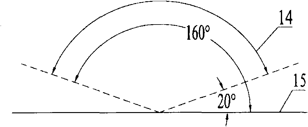
[0052] The angle between the flexible fiber axis and the working surface in the flexible nano-brush layer tends to be 90°.

[0053] Its preparation method comprises the following steps:

[0054] (1) Anodic oxidation is used to produce an alumina template with an average pore diameter of 200nm, a depth of 60μm, and a hole center distance of ≈270nm; the angle between the axis of the hole and the surface of the template is 90°, that is, the axis of the hole is perpendicular to the surface of the template...

Embodiment 2

[0063] A kind of flexible nano-brush polishing pad, is made up of flexible nano-brush layer 11, matrix layer 12 and elastic substrate layer 13, groove is arranged on the surface of nano-brush polishing pad, flexible nano-brush layer 11 working surface has the flexible fiber of following characteristics:

[0064] Diameter: ≈80nm;

[0065] Spacing (referring to the center distance of the axis of the fiber root): ≈120nm;

[0066] Length: ≈160nm;

[0067] Length-to-diameter ratio: ≈2:1.

[0068] The angle between the flexible fiber axis and the working surface in the flexible nano-brush layer tends to be 90°.

[0069] The method for making the above-mentioned flexible nano brush polishing pad with grooves may further comprise the steps:

[0070] (1) Anodic oxidation is used to produce an alumina template with an average pore diameter of 80nm, a depth of 10μm, and a hole center distance of ~120nm. The size of the template is 10mm×10mm, and the angle between the axis of the hole ...

Embodiment 3

[0077] A flexible nano-brush polishing pad, without grooves and holes on the surface, is composed of a flexible nano-brush layer 11 and a base layer 12, and the flexible nano-brush layer 11 has a flexible fiber with the following characteristics on the working surface:

[0078] Diameter: 10μm;

[0079] Pitch: 10μm;

[0080] Length: 20μm;

[0081] Length-to-diameter ratio: 2:1.

[0082] The angle between the axis of the flexible fibers in the flexible nano-brush layer and the working surface is 60°.

[0083] Its preparation method comprises the following steps:

[0084] (1) Process a porous silicon template with an average pore diameter of 10 μm, a spacing of 10 μm, and a depth of 20 μm on the surface of the silicon wafer by plasma dry etching method DRIE; the angle between the axial direction of the hole and the surface of the template is 60°;

[0085] (2) Prepare a treated clean and smooth polyurethane plate (Shore hardness: 65D) as the base layer 12;

[0086] (3) dissol...


PUM


Abstract

The invention discloses a polishing pad for chemical mechanical planarization (CMP) and a manufacturing method thereof, and belongs to the technical field of a chemical mechanical planarization process. The polishing pad comprises a base layer on which a flexible nanometer brush layer is arranged. The nanometer brush polishing pad is prepared by the following steps of: preparing a template, coating polymer solution on the base layer and transferring a nanometer structure on the template to the base layer. Compared with the prior art, the polishing pad has the most outstanding advantage of having a flexible fiber structure; the polishing pad realizes material removal when in flexible contact with a polished surface, can solve the stress problem in the conventional chemical mechanism planarization technique to the largest degree, and is applicable to CMP under ultra-low pressure. Moreover, the polishing pad can overcome the defects of a relatively hard polishing pad such as scratch, over-polishing, butterfly, corrosion and the like, and a higher-quality polished surface can be obtained. The polishing pad has the advantages of simple manufacturing method, high controllability of the technical process and stable polishing performance.

Description

technical field [0001] The present invention relates to a chemical mechanical planarization process in the field of semiconductor integrated circuit manufacturing, in particular to a polishing pad that can be used for chemical mechanical planarization, and more specifically, the present invention relates to a polishing pad for chemical mechanical planarization and its method of manufacture. Background technique [0002] Chemical Mechanical Planarization / Polishing (CMP for short) is considered to be the most effective method to achieve global planarization at present. As an ancient process, CMP was originally used to polish glass. In the 1980s, IBM first applied CMP to the microelectronics manufacturing process. SiO 2 Since then, it has developed very rapidly. At present, the application of CMP has been extended to metals (such as Al, Cu, Ti, Ta, W, etc.), dielectrics (such as SiO 2 、Si 3 N 4 , various Low-k materials, etc.), polysilicon, ceramics, magnetic disks, magneti...

Claims


Application Information

Patent Timeline
Patent Type & Authority Patents(China)
IPC IPC(8): B24D13/00B24D18/00
Inventor 雒建斌韩桂全刘宇宏路新春
Owner TSINGHUA UNIV
Learn More