Method for preparing wafer-level uniform-dimension glass microcavity by positive pressure thermal forming

A wafer-level, thermoforming technology, used in manufacturing tools, welding equipment, microstructure technology, etc., can solve the problems of increased cost, high cost, long time, etc., and achieve the effect of low cost, good sphericity, and simple method.

Active Publication Date: 2010-12-08
SOUTHEAST UNIV
View PDF3 Cites 10 Cited by
  • Summary
  • Abstract
  • Description
  • Claims
  • Application Information

AI Technical Summary

Problems solved by technology

These methods are more complex and costly
Using DRIE etching also takes a long time, further increasing the cost

Method used


Image

  • Method for preparing wafer-level uniform-dimension glass microcavity by positive pressure thermal forming
  • Method for preparing wafer-level uniform-dimension glass microcavity by positive pressure thermal forming
  • Method for preparing wafer-level uniform-dimension glass microcavity by positive pressure thermal forming

Examples


Embodiment 1

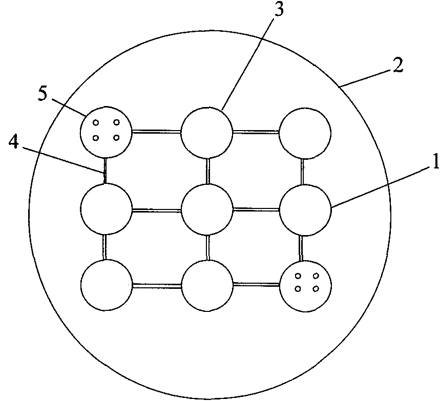
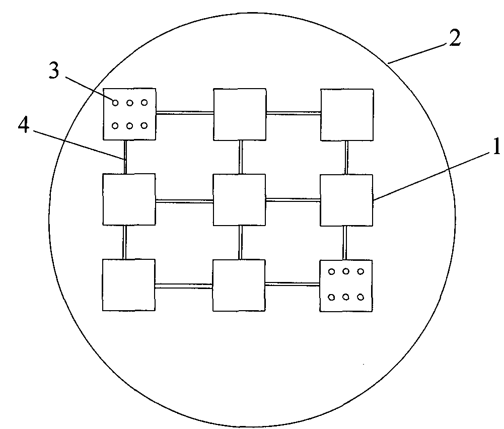
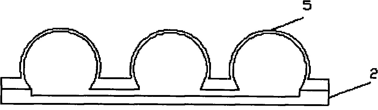
[0023]A kind of method that positive pressure thermoforming prepares the glass microcavity of disc level uniform size, comprises the following steps: engrave the array (the size of microgroove is identical) that same microgroove forms on silicon wafer, the method for etching microgroove can be Dry method and wet method, preferably wet method (the depth of the microgroove required by the present invention can place the heat release agent, so the shallower depth of wet etching can meet the requirements, such as the depth of 50-100 microns) , the etched microgrooves have the same size (for example, 5, 10, 15, 50), microchannels are engraved between the microgrooves, and the minimum groove width of the microgrooves is greater than 5 times of the flow channel width. Place an appropriate amount of heat release agent in at least one microgroove (can place heat release agent in two or more microgrooves, the consumption of heat release agent is calculated according to the volume space o...

Embodiment 2

[0026] A method for preparing a wafer-level uniform-sized glass microcavity by positive pressure thermoforming, comprising the following steps:

[0027] The first step is to oxidize a 5000A oxide layer on a single-sided polished silicon wafer by a combination of dry and wet oxygen, spin-coat AZ P4620 photoresist on the polished surface, expose and develop to remove the photoresist that needs to be etched on the surface of the microgroove. Utilize the Si micromachining process to etch the microcavity and the microchannel shallow groove on the 4-inch Si wafer, and the microchannel connects the shallow groove. The silicon wafer used can be a standard thickness silicon wafer with a thickness of 500 microns. The depth of the groove is 60-100 microns, the micro-groove is a square groove with a width of 2000 microns, and the micro-channel used to connect two micro-grooves is a strip-shaped groove with a width of 50 microns. Square groove, the micromachining process of the pattern str...

Embodiment 3

[0033] A method for preparing a wafer-level uniform-sized glass microcavity by positive pressure thermoforming, comprising the following steps:

[0034] The first step is to oxidize a 5000A oxide layer on a single-sided polished silicon wafer by a combination of dry and wet oxygen, spin-coat AZ P4620 photoresist on the polished surface, expose and develop to remove the photoresist that needs to be etched on the surface of the microgroove. Utilize Si micromachining process to etch microgrooves and microchannels on 4-inch Si wafers, microchannels connect microgrooves, used silicon wafers can be silicon wafers of standard thickness, and thickness is 500 microns, and the depth of described microgrooves is 60-100 microns, square groove with a width of 2000 microns, the number of micro-grooves is 15, the size is the same, the micro-channel groove is a strip-shaped groove with a diameter of 50 microns, and the length of the groove is 5 mm, connecting two adjacent microcavity squares ...


PUM

PropertyMeasurementUnit
depthaaaaaaaaaa
diameteraaaaaaaaaa

Abstract

The invention discloses a method for preparing a wafer-level uniform-dimension glass microcavity by positive pressure thermal forming. The method comprises the following steps of: etching an array consisting of microgrooves on a silicon wafer, and etching microchannels connecting the microgrooves, wherein the minimum groove width of the microgrooves is 5 times more than the runner width; and putting a proper amount of thermal outgassing agent into at least one microgroove, correspondingly bonding the plurality of microgrooves to form a sealed cavity by using a glass wafer, heating to soften the glass, making the thermal outgassing agent heated to release gases to generate positive pressure, acting the positive pressure on the softened glass corresponding to the plurality of microgrooves which are connected through the microchannels so as to form a spherical microcavity with uniform dimension, and cooling the microcavity. By connecting the same microgrooves through the microchannel, the inside air pressure of the microgrooves is substantially consistent, and the formed glass microcavity has uniform dimension. When the dimension of the microgrooves is far greater than that of the microchannel, the microchannels with smaller radius hardly expand due to higher additional pressure. Therefore, the glass corresponding to the microchannels can keep smooth.

Description

technical field [0001] The invention relates to a MEMS (micro-electro-mechanical system) manufacturing technology, in particular to a method for preparing a wafer-level uniform-sized glass microcavity by positive pressure thermoforming. Background technique [0002] In the field of MEMS manufacturing technology, Pyrex7740 glass (a glass containing alkaline ions, Pyrex is Corning's product brand) is an important material. It has a thermal expansion coefficient similar to that of Si materials, and has high light transmittance. High strength, and can form a high-strength bonding connection with the Si substrate by using the anodic bonding process, and a strong Si-O covalent bond is generated on the bonding surface, and its strength is even higher than that of the Si material itself. Due to such characteristics, Pyrex7740 glass is widely used in MEMS packaging, microfluidics and MOEMS (micro-optical electro-mechanical systems) and other fields. [0003] In the field of MEMS pac...

Claims


Application Information

Patent Timeline
Patent Type & Authority Applications(China)
IPC IPC(8): B81C3/00
Inventor 尚金堂陈波寅张迪徐超
Owner SOUTHEAST UNIV
Why Eureka
Try Eureka