Method for passivating back of crystal silicon solar cell

A solar cell and backside passivation technology, which is applied in the field of solar photovoltaic utilization, can solve the problems of poor long-wave response of the battery, unfavorable components, and bending of the battery sheet, and achieve the effects of reducing the recombination rate, reducing the bending, and enhancing the back reflection

Inactive Publication Date: 2010-12-15
JA SOLAR
View PDF5 Cites 21 Cited by
  • Summary
  • Abstract
  • Description
  • Claims
  • Application Information

AI Technical Summary

Problems solved by technology

SiNx has a good passivation effect, but there is no passivation measure on the back side, so the recombination is serious, resulting in poor long-wave response of the battery
And with the further thinning of the silicon wafer, the adverse effect of th

Method used


Image

  • Method for passivating back of crystal silicon solar cell
  • Method for passivating back of crystal silicon solar cell
  • Method for passivating back of crystal silicon solar cell

Examples


Embodiment 1

[0023] figure 2 , 3 Shown is the specific preparation process of the embodiment of the present invention:

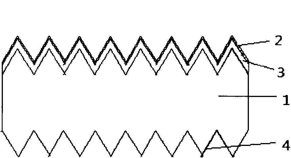
[0024] (1) making a suede surface after removing the surface damage layer of the silicon wafer 1;

[0025] (2) Diffusion of P in POCl3 atmosphere to form n + diffusion layer;

[0026] (3) Deposit SiNx antireflection film 2 on the front side of silicon wafer 1 with PECVD;

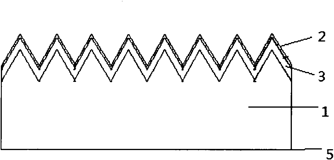
[0027] (4) Corroding the back side of the solar cell in 20% sodium hydroxide solution at 70° C. for 15 minutes to obtain a polished surface 5;

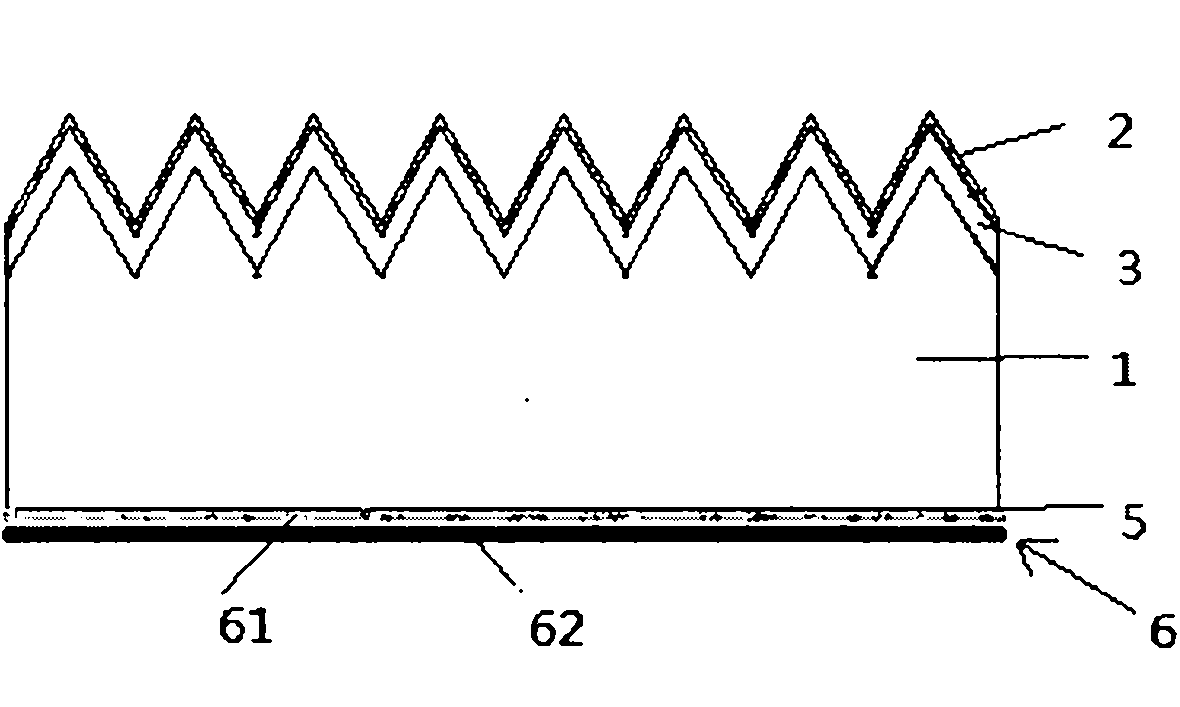
[0028] (5) Deposit SiO on the polished surface 5 2 / SiNx (passivation layer 61 / passivation layer 62) forms the back passivation layer 6;

[0029] (6) Utilize laser etching or screen printing corrosive paste to open an electrode window on the back passivation layer 6;

[0030] (7) screen printing back electrode and positive electrode;

[0031] (8) Sintering in a sintering furnace to form an ohmic contact;

[0032] (9) Test sorting.

Embodiment 2

[0034] figure 2 , 3 Shown is the specific preparation process of the embodiment of the present invention:

[0035] (1) making a suede surface after removing the surface damage layer of the silicon wafer 1;

[0036] (2) Diffusion of P in POCl3 atmosphere to form n + diffusion layer;

[0037] (3) Deposit SiNx antireflection film 2 on the front side of silicon wafer 1 with PECVD;

[0038] (4) Corroding the back side of the solar cell in 30% potassium hydroxide solution at 80° C. for 12 minutes to obtain a polished surface 5;

[0039] (5) Deposit SiC / SiNx (passivation layer 61 / passivation layer 62) on the polishing surface 5 to form a back passivation layer 6;

[0040] (6) Utilize laser etching or screen printing corrosive paste to open an electrode window on the back passivation layer 6;

[0041] (7) screen printing back electrode and positive electrode;

[0042] (8) Sintering in a sintering furnace to form an ohmic contact;

[0043] (9) Test sorting.

Embodiment 3

[0045] figure 2 , 3 Shown is the specific preparation process of the embodiment of the present invention:

[0046] (1) making a suede surface after removing the surface damage layer of the silicon wafer 1;

[0047] (2) Diffusion of P in POCl3 atmosphere to form n + diffusion layer;

[0048] (3) Deposit SiNx antireflection film 2 on the front side of silicon wafer 1 with PECVD;

[0049] (4) Corroding the back side of the solar cell for 10 minutes in a 20% tetramethylammonium hydroxide solution at 80° C. to obtain a polished surface 5;

[0050] (5) Deposit a-Si / SiO on the polished surface 5 2 (passivation layer 61 / passivation layer 62) forming a back passivation layer 6;

[0051] (6) Utilize laser etching or screen printing corrosive paste to open an electrode window on the back passivation layer 6;

[0052] (7) screen printing back electrode and positive electrode;

[0053] (8) Sintering in a sintering furnace to form an ohmic contact;

[0054] (9) Test sorting.


PUM


Abstract

The invention discloses a method for passivating the back of a crystal silicon solar cell. The method comprises the following steps of: depositing a SiN* anti-reflection film on the front of the solar cell, corroding the back of the solar cell in heated alkali liquor by using the SiN* anti-reflection film as a mask to obtain a polished surface required by passivation, then depositing double film passivation layers on the polished surface to form a back passivation layer, forming an electrode window on the back passivation layer by adopting laser etching or screen printing of corrosive slurry, and finally forming a local contact back electrode on the electrode window by adopting a screen printing or sputtering method. The method greatly improves the long wave response of the solar cell and improves the conversion efficiency of the solar cell; moreover, a full-aluminum back field structure is canceled, so the method reduces the bending of the solar cell and is more adaptive to the thinning tendency of the solar cell.

Description

technical field [0001] The invention relates to the technical field of photovoltaic utilization of solar energy, in particular to a preparation method of a crystalline silicon solar cell. Background technique [0002] The current commercial solar cell production process is simple and the manufacturing cost is relatively low. Its production process: remove the damaged layer on the surface of the silicon wafer, make texture → in POCl 3 Diffusion of P in the atmosphere to form n + Diffusion layer → use plasma etching or wet etching to remove the PN junction around the silicon wafer → use PECVD technology to deposit SiNx anti-reflection film on the front → screen print the back electrode, back electric field, and positive electrode → form by sintering in a sintering furnace Ohmic contact → test sorting. This commercial solar cell manufacturing technology is relatively simple, low in cost, suitable for industrialized and automated production, and thus widely used. However, th...

Claims


Application Information

Patent Timeline
IPC IPC(8): H01L31/18
CPCY02P70/50
Inventor 尹海鹏朱生宾何胜金井升单伟
Owner JA SOLAR
Why Eureka
Try Eureka