A kind of preparation method of se solar cell

A technology of solar cells and products, applied in the direction of circuits, photovoltaic power generation, electrical components, etc., can solve the problems of not being able to meet the protection of PSG masks, restricting the application of alkali polishing on the back, and affecting the structure of SE cells, etc., to increase back reflection and back Passivation effect, improve the quality of SE battery, increase the effect of low-temperature phosphorus diffusion

Active Publication Date: 2022-04-12
TIANJIN AIKO SOLAR ENERGY TECH CO LTD
View PDF9 Cites 0 Cited by
  • Summary
  • Abstract
  • Description
  • Claims
  • Application Information

AI Technical Summary

Problems solved by technology

[0003] At present, SE cells are mainly realized by laser doping, that is, the phosphorus atoms in the thermally diffused PSG are redistributed by secondary diffusion through laser energy. However, this method has the following defects: the PSG located at the laser doping position It will be destroyed and cannot meet the PSG mask protection. In the back alkali polishing process, the front laser doped position will be partially polished by the alkali solution because there is no PSG or SiO2 layer, which will affect the structure of the SE battery and also restrict the back alkali polishing. app promotion for

Method used


Image

  • A kind of preparation method of se solar cell
  • A kind of preparation method of se solar cell

Examples


Embodiment Construction

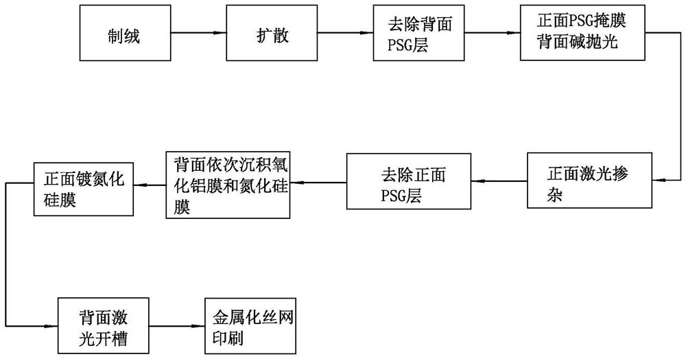
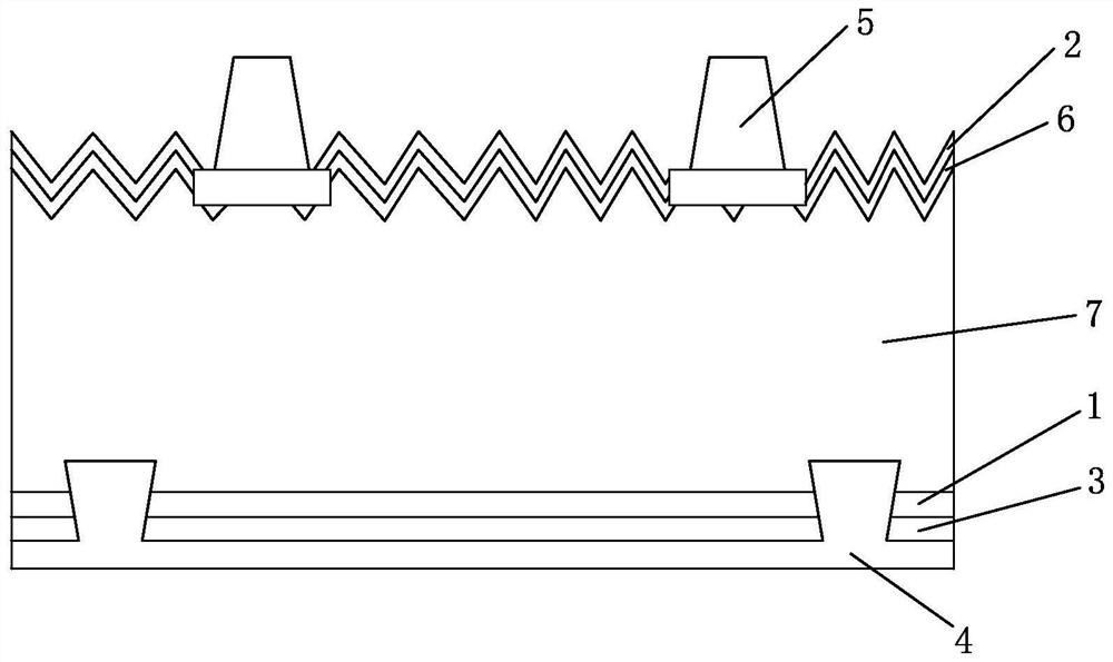
[0038] Such as figure 1 and 2 Shown, is the preparation method of a kind of SE solar cell of the present invention, specifically comprises the following steps:

[0039] S1. Select a lightly doped p-type single crystal silicon wafer 7 (P-type silicon) with a resistivity of 0.1-6Ω·cm, and perform alkali texturing on the P-type silicon to form pyramid-shaped anti-reflection on the front and back sides For the suede surface, the weight loss range of velvet making is 0.4-0.8g, and the reflectivity (full band 300-12000nm) range is 10%-18%.

[0040] S2. Place the product obtained in step S1 in a furnace tube at 500-900° C. for P (phosphorus) diffusion for 5 minutes to 30 minutes to form a PSG layer on the surface of the silicon wafer, that is, to form an N-type emitter 6, and then perform low-temperature P (phosphorus) diffusion. (phosphorus) diffusion, to ensure that there is a certain proportion of phosphorus atoms in PSG, and to provide phosphorus source for laser doping.

[00...


PUM

PropertyMeasurementUnit
thicknessaaaaaaaaaa
thicknessaaaaaaaaaa
thicknessaaaaaaaaaa

Abstract

The invention discloses an alkali polishing method for an SE battery. P-type silicon is made into cashmere; phosphorus is diffused to form a PSG layer on the surface of a silicon chip, that is, an N-type emitter is formed; the oxidation time is 5min-30min, and the oxygen flow rate is 1000-5000slm / min; Protect the front PSG layer and remove the back PSG layer; alkali polish the back to protect the front PSG layer from corrosion; use the front PSG layer as an impurity source for laser doping, and then remove the front PSG layer; deposit aluminum oxide film on the back; Silicon nitride anti-reflection coating on the back; laser groove on the back; back electrode printed on the back; aluminum back field printed on the back; positive electrode printed on the front; high temperature sintering. In the backside alkali polishing process of the present invention, the front laser-doped position is protected by the PSG layer, and will not be partially polished by the alkali solution, thereby ensuring the SE battery structure and improving the SE battery quality, so that the backside alkali polishing process can be popularized and applied.

Description

technical field [0001] The invention relates to a preparation method of an SE solar cell. Background technique [0002] The development direction of solar cells is low cost and high efficiency. Selective emitter technology (selective emitter, SE) is one of the methods that are expected to achieve high efficiency in the production process of crystalline silicon solar cells. SE solar cells refer to high-concentration doping at and near the contact between metal grid lines and silicon wafers, and low-concentration doping in areas other than electrodes. Such a structure not only reduces the contact resistance between the silicon wafer and the electrode, but also reduces the surface recombination, improves the minority carrier lifetime, and improves the short-circuit current, open-circuit voltage and fill factor, thereby improving the conversion efficiency. [0003] At present, SE cells are mainly realized by laser doping, that is, the phosphorus atoms in the thermally diffused ...

Claims


Application Information

Patent Timeline
Patent Type & Authority Patents(China)
IPC IPC(8): H01L31/18H01L31/0216H01L31/0236C01B33/10
CPCH01L31/1876H01L31/02167H01L31/02363C01B33/10Y02E10/50Y02P70/50
Inventor 李吉赵朋松顾生刚杨二存夏利鹏赵本定刘海金赵小平胡番
Owner TIANJIN AIKO SOLAR ENERGY TECH CO LTD
Why Eureka
Try Eureka