A kind of n-type silicon solar cell and its preparation method
A technology of solar cells and n-type silicon, which is applied in the field of solar cells, can solve the problems of low conversion efficiency, achieve the effects of increasing life, increasing open circuit voltage, and reducing manufacturing costs
- Summary
- Abstract
- Description
- Claims
- Application Information
AI Technical Summary
Problems solved by technology
Method used
Image
Examples
Embodiment 1
[0032] Embodiment 1, an n-type silicon solar cell.
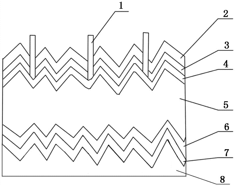
[0033] like figure 1 As shown, the n-type silicon solar cell provided in this embodiment includes an n-type silicon substrate 5, and a p-doped layer 4, a front passivation layer 3 and Reflective layer 2, the material adopted in front passivation layer 3 is silicon oxide (SiO 2 ) or silicon nitride (Si 3 N 4 ). The front electrode 1 is prepared by screen printing and sintering process, and the front electrode 1 passes through the anti-reflection layer 2 and the front passivation layer 3 and is in contact with the p-doped layer 4 .
[0034] On the back side of the n-type silicon substrate 5, an n is formed by doping + doped layer 6, the n + The back passivation layer 7 is formed on the doping layer 6, and the main material of the back passivation layer 7 is a ferroelectric thin film material. The ferroelectric thin film material can be, for example, lead zirconate titanate (PZT), barium titanate (BTO), iron Bismuth oxid...
Embodiment 2
[0035] Embodiment 2, a preparation method of an n-type silicon solar cell.
[0036] The preparation method of the n-type silicon solar cell provided in this embodiment comprises the following steps:
[0037] ①. Select an n-type silicon substrate, and clean the selected n-type silicon substrate. After cleaning, texture the front and back of the n-type silicon substrate, so that the front and back of the n-type silicon substrate form a pyramid-like texture. surface structure. The average height of the pyramids in the suede structure is generally controlled between 1 μm and 15 μm.
[0038] ②. Phosphorus is used to form a heavily doped n+ doped layer on the back of the n-type silicon substrate, and then cleaned to remove PSG (phosphosilicate glass); boron is diffused on the front of the n-type silicon substrate to obtain p-doping layer, thereby forming a pn junction, and then cleaning to remove BSG (borosilicate glass).
[0039] ③. A front passivation layer is prepared on the p...
Embodiment 3
[0056] Compared with embodiment 2, this embodiment adds a step after step ① and before step ②: planarizing the back side of the n-type silicon substrate. In this embodiment, the step of "planarizing the back of the n-type silicon substrate" is added, the purpose of which is to process the pyramid-shaped back into a slightly smooth back, that is, to smooth the top tip of the pyramid, so that the pyramid The apex-like structure of the structure and the sharp-edged horn-like structure at the bottom of the valley become smooth, and at the same time, the surface of the pyramid changes from rough to relatively smooth. After planarizing the back of the n-type silicon substrate, it should be ensured that natural local contacts can still be formed after the subsequent formation of the back passivation layer, which is convenient for subsequent direct preparation of the full back metal film as the back electrode.
[0057] In this embodiment, the back surface of the n-type silicon substra...
PUM
 Abstract
Description
Claims
Application Information


