Masking method for deep-etching multi-layer silicon structure by dry method

A silicon structure, multi-layer silicon technology, applied in microstructure technology, microstructure devices, manufacturing microstructure devices, etc., can solve problems such as poor dimensional accuracy, structural sidewall and edge deformation, and achieve perfect edge structure and dimensional accuracy. High, process repeatability effect

Inactive Publication Date: 2011-04-06
TIANJIN SEAGULL WATCH CO LTD +1
View PDF2 Cites 6 Cited by
  • Summary
  • Abstract
  • Description
  • Claims
  • Application Information

AI Technical Summary

Problems solved by technology

[0005] The disadvantage of this method is that if Figure 3a to Figure 3b It is a schematic diagram of sidewall and edge defects generated during multilayer structure etching. When multilayer structure is etched, the surface of the structure is completely exposed to plasma and directly bombarded by ions, so the dimensional accuracy is poor, and the sidewall and edge of the structure are seriously deformed.

Method used


Image

  • Masking method for deep-etching multi-layer silicon structure by dry method
  • Masking method for deep-etching multi-layer silicon structure by dry method
  • Masking method for deep-etching multi-layer silicon structure by dry method

Examples


Embodiment

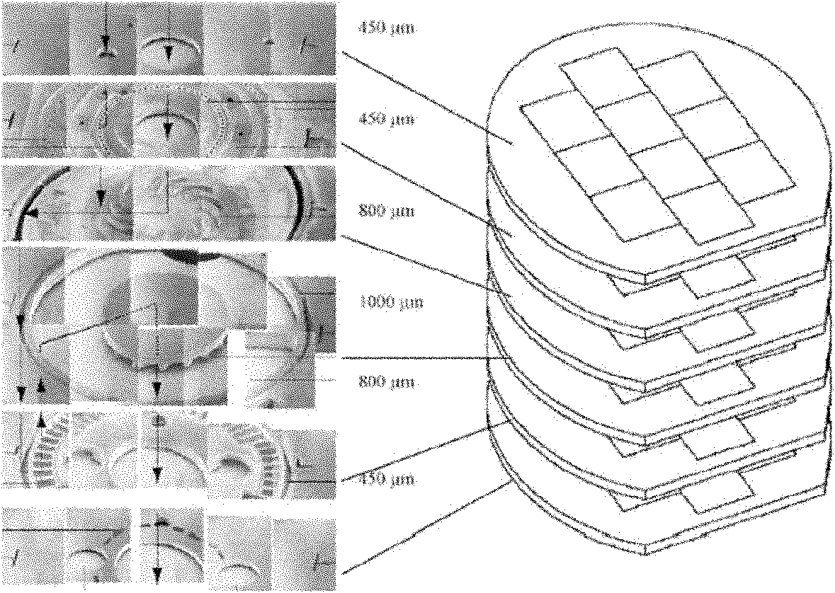
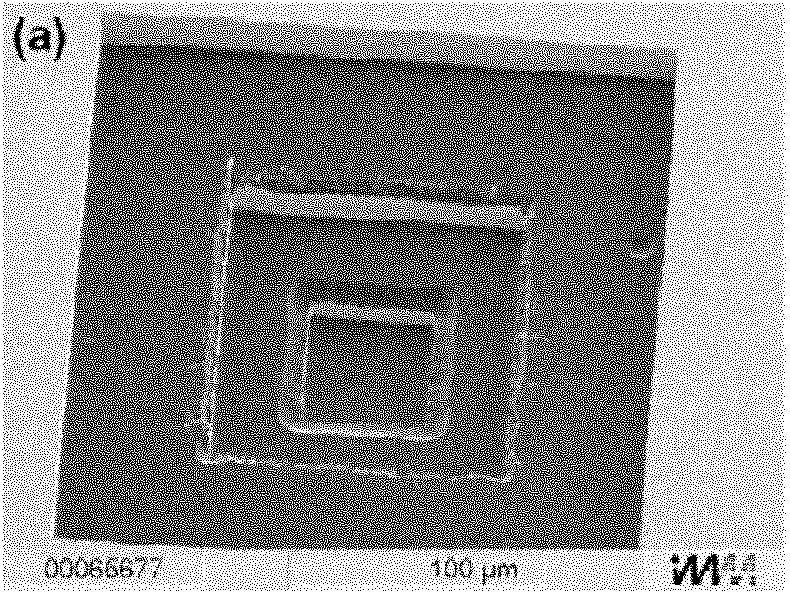
[0063] FIG. 7 is a process flow chart of specific steps 1 to 13 of a novel multilayer silicon dry deep etching mask.

[0064] In the figure: 7a to 7m represent steps 1 to 13 respectively.

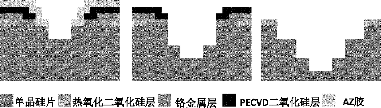
[0065] Step 1: Select a suitable monocrystalline silicon wafer (4 inches, 400um thick, )

[0066] a) RCA2 wash-DI:H 2 o 2 : HCL=10:2:1; 50°C, 15-20mins.

[0067] b) Wafer container: Teflon cassette

[0068] c) Equipment: fume hood

[0069] Step 2: Apply Az4620P photoresist

[0070] a) 15s, 600rpm; 25s, 3000rpm. (7.3um thickness)

[0071] b) Equipment: Spin coater KW-4A homogenizer

[0072] Step 3: UV lithography to obtain the first layer mask

[0073] a) 1.7mw / cm 2 x 60s=102mJ / cm 2

[0074] b) Equipment: Karl Suss MA4, 400nm

[0075] Step 4: DRIE etching the first layer structure

[0076] a) Process conditions: Table 2, 40 cycles

[0077] b) Equipment: Oxford PlasmaLab 100etcher

[0078] c) Depth of etching structure: 50um

[0079] Step 5: Clean the residual Az photoresist m...


PUM


Abstract

The invention discloses a masking method for deep-etching a multi-layer silicon structure by a dry method. The masking method comprises the following steps of: A, photoetching an Az positive photoresist pattern; B, performing the deep-etching on a silicon structure by taking the obtained Az positive photoresist pattern as a mask; C, cleaning the Az mask and the silicon structure, and coating a first layer of Su8 negative photoresist; D, photoetching the Su8 photoresist to obtain a mask pattern of a lower structure by an alignment mark; and E, deep-etching a lower silicon structure by taking the pattern obtained from the step D as the mask; and repeating the steps to obtain the multi-layer silicon microstructure with greater structure depth. The method has the advantages that: because the Su8 photoresist is selected as the mask for deep reactive ion etching of the inductively coupled plasmas, an effect of protecting an etched structure is achieved and the direct physical bombardment of ions caused by exposing a previous etching structure in the plasmas is effectively avoided; and the method has high process repeatability, can be used in the same component repeatedly and realizes three or more layers of monocrystalline silicon microstructures with a high aspect ratio.

Description

technical field [0001] The invention relates to a method for dry etching a silicon wafer in the microfabrication field; in particular, it relates to a mask method for deep etching a multilayer silicon structure by using a dry method. Background technique [0002] One of the greatest advances of mankind in the last century is the development of microelectronics technology. Along with the development of microelectronics technology, a brand-new technology——MEMS (Micro Electromechanical System, that is, Micro Electromechanical System) was quietly born and began to develop rapidly. Micro Electro Mechanical Systems (MEMS for short) is the use of modern micro-processing technology (including silicon micromachining, silicon surface micromachining, LIGA and other technologies), the mechanical components, optical systems, drive components, electronic control systems Integrated into complex systems such as sensors, actuators, and drives with excellent performance, low price, and minia...

Claims


Application Information

Patent Timeline
Patent Type & Authority Applications(China)
IPC IPC(8): B81C1/00G03F7/00
Inventor 郭育华王英男江争马广礼
Owner TIANJIN SEAGULL WATCH CO LTD
Why Eureka
Try Eureka