

Substrate with oxide layer and manufacturing method thereof
A technology of oxide layer and manufacturing method, which is applied in the manufacture of discharge tubes/lamps, manufacturing tools, cold cathode manufacturing, etc., can solve the problems of difficult application, high durability of chemical corrosion, etc., to reduce production costs, inhibit damage, improve Effects on productivity and processing quality
- Summary
- Abstract
- Description
- Claims
- Application Information
AI Technical Summary
Problems solved by technology
Method used
Image

Examples
example 1
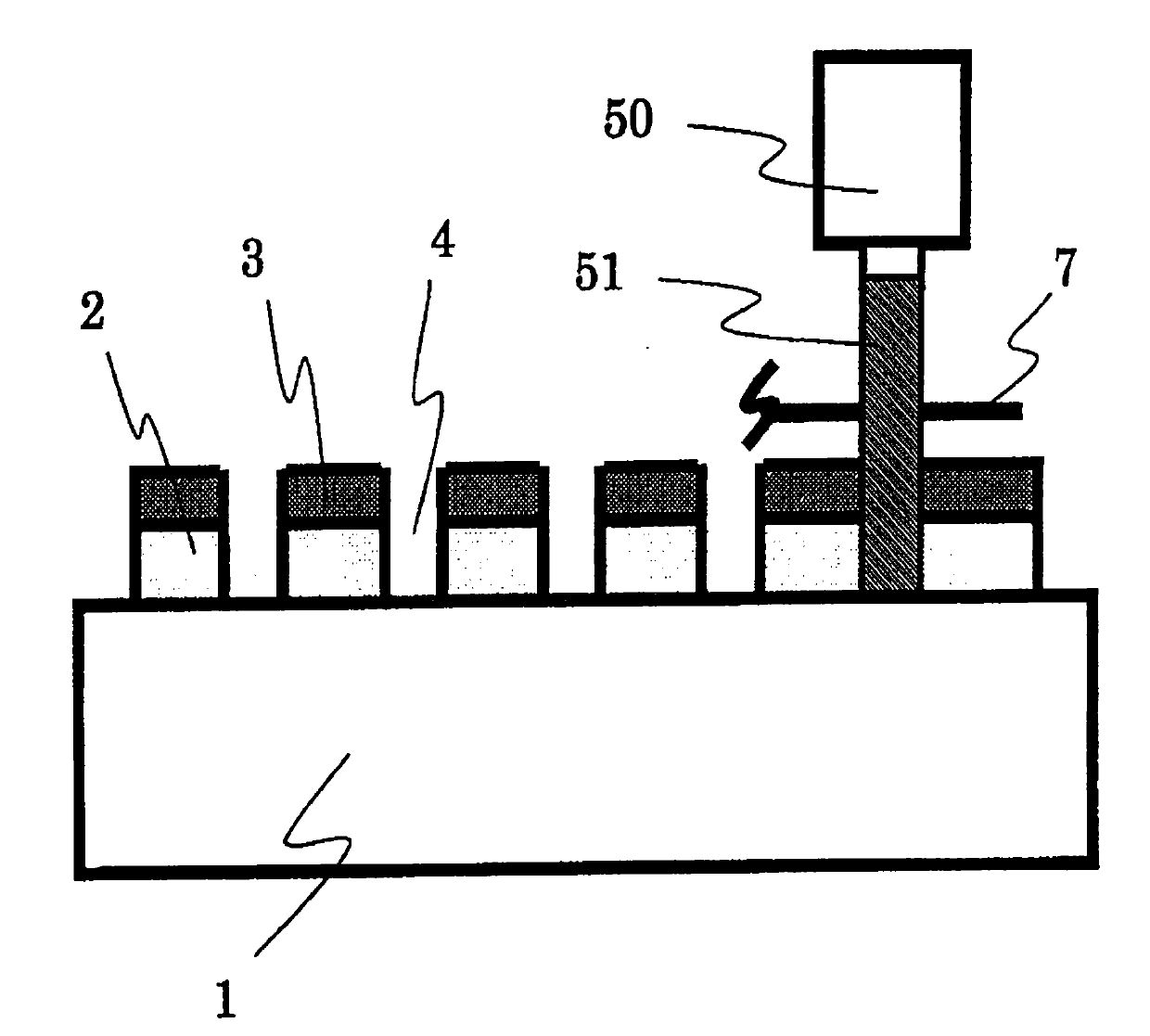
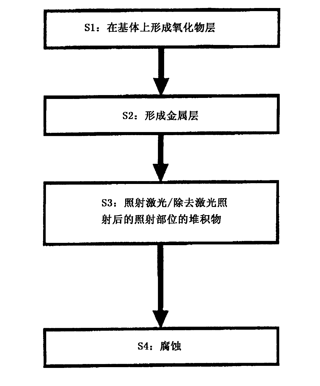
[0098] A PDP with a thickness of 2.8 mm x a length of 100 mm x a width of 100 mm was cleaned with a substrate of high strain point glass (PD200 manufactured by Asahi Glass Co., Ltd.), and then set as a substrate in a sputtering apparatus. By DC magnetron sputtering method, using ITO (relative to In 2 o 3 with SnO 2 The total amount contains 10% by mass of SnO 2 ) target, and an ITO layer with a thickness of 120 nm was formed on the substrate to obtain a glass substrate with an ITO layer. The sputtering gas used contained 2 vol% O 2 Gas Ar gas. Back pressure is 1×10 -3 Pa, sputtering gas pressure is 0.4Pa, power density is 3.5W / cm 2 . In addition, the substrate temperature was 250°C.
[0099] The glass substrate with the ITO layer was irradiated with pulsed laser light from the ITO layer side. As the pulsed laser, pulsed laser light (wavelength: 1064 nm) emitted from a pulsed Yb-fiber laser was used. This pulsed laser has a Gaussian energy distribution 6, and the powe...
example 2
[0103] On the ITO layer of the glass substrate with the ITO layer of Example 1, after exhausting the residual gas, an auxiliary layer with a thickness of 11 nm was formed by DC magnetron sputtering using a Cr metal target in an Ar gas atmosphere. Back pressure is 1×10 -3 Pa, sputtering gas pressure is 0.3Pa, input power density is 1W / cm 2 . In addition, the substrate temperature was 250°C.
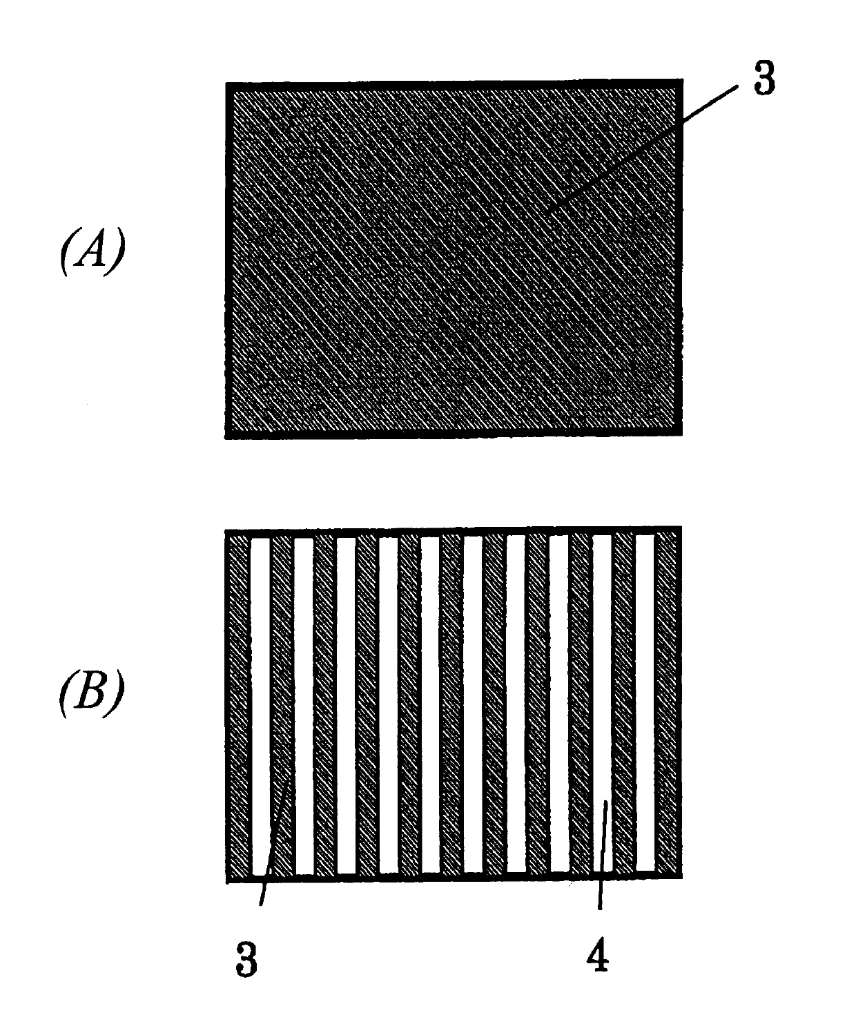
[0104] The glass substrate with an auxiliary layer of this example was irradiated with the same pulsed laser light as in Example 1 from the film surface side. Then, in order to evaluate the pattern diameter of the ITO layer, the auxiliary layer on the entire surface of the substrate was removed with an etchant. A mixture of cerium ammonium nitrate, perchloric acid and water is used as the etching solution. Substantial damage was not observed on the ITO layer by the etchant treatment.
[0105] The pattern diameter of the ITO layer of this example was evaluated with an optical microscop...
example 3
[0107] On the glass substrate used in example 1, utilize direct current magnetron sputtering method, use the 2 o 5 SnO and ZnO 2 Target (contains 96% by mass Ta relative to the total amount 2 o 5 , 0.5% by mass ZnO), forming SnO with a thickness of 140nm 2 layer, obtained with SnO 2 layers of glass substrates.
[0108] The sputtering gas used contained 2 vol% O 2 Gas Ar gas. Back pressure is 1×10 -3 Pa, sputtering gas pressure is 0.4Pa, power density is 3.5W / cm 2 . In addition, the substrate temperature was 250°C.
[0109] In this example with SnO 2 The same pulsed laser as in Example 1 was irradiated from the film surface side on the glass substrate of the layer, and the pattern diameter was measured by the same method as in Example 1. The results are shown in Table 1.
PUM
| Property | Measurement | Unit |
|---|---|---|
| Energy density | aaaaa | aaaaa |
| Pulse width | aaaaa | aaaaa |
| Wavelength | aaaaa | aaaaa |
Abstract
Description
Claims
Application Information