Dielectric film, dielectric element, and process for producing the dielectric element

A manufacturing method and technology of dielectric components, applied in semiconductor/solid-state device manufacturing, electrical components, semiconductor devices, etc., to achieve the effects of avoiding substrate interface degradation, easy operation, and low cost

Inactive Publication Date: 2011-04-27
NAT INST FOR MATERIALS SCI
View PDF7 Cites 5 Cited by
  • Summary
  • Abstract
  • Description
  • Claims
  • Application Information

AI Technical Summary

Problems solved by technology

[0004] Based on the above background, the present invention solves the existing problems, and provides a method that can achieve high dielectric constant and good insulation characteristics at the same time even in the nanometer field, and can operate at low temperatures without the influence of substrate interface degradation and composition deviation. A new technical method for component fabrication

Method used


Image

  • Dielectric film, dielectric element, and process for producing the dielectric element
  • Dielectric film, dielectric element, and process for producing the dielectric element
  • Dielectric film, dielectric element, and process for producing the dielectric element

Examples


Embodiment 1

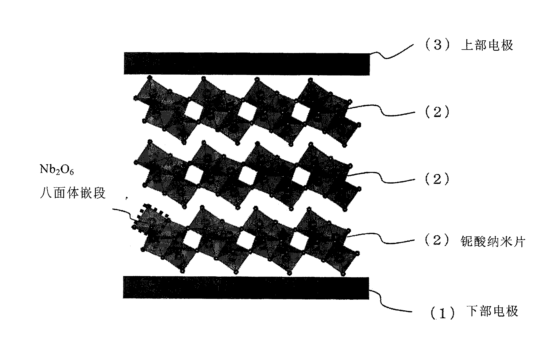
[0063] In this embodiment, layered niobium oxide (such as KTiNbO 5 ) as the starting material to make niobic acid nanosheets (2), such as figure 1 As shown, fabricated in atomically flat epitaxy SrRuO as follows 3 The substrate (1) alternately has the above-mentioned niobic acid nanosheets (2) and the multilayer film of cationic polymer (4) polyethyleneimine (PEI).

[0064] layered niobium oxide (KTiNbO 5 ) is obtained as follows, potassium carbonate (K 2 CO 3 ), titanium oxide (TiO 2 ) and niobium oxide (Nb 2 o 5 ) were mixed at a ratio of K:Ti:Nb of 1.05:2:1, calcined at 900° C. for 1 hour, and then calcined at 1100° C. for 20 hours.

[0065] 1 g of this powder was subjected to acid treatment in 100 mL of a predetermined 1 hydrochloric acid aqueous solution at room temperature to obtain a hydrogen exchange body (HTiNbO 5 ), then, add tetrabutylammonium hydroxide (hereinafter referred to as TBAOH) aqueous solution 100mL in 0.4g of this hydrogen exchange body, stir at ...

Embodiment 2

[0079] In this embodiment, layered niobium oxide (such as KTiNbO 5 ) as the starting material to produce niobate nanosheets (TiNbO 5 ),Such as figure 1 As shown, the atomically planar epitaxial SrRuO used as the lower electrode substrate 3 A multilayer film of the above-mentioned niobate nanosheets (2) was produced on the substrate (1) by the LB method (Langmuir-Blodgett method) as follows.

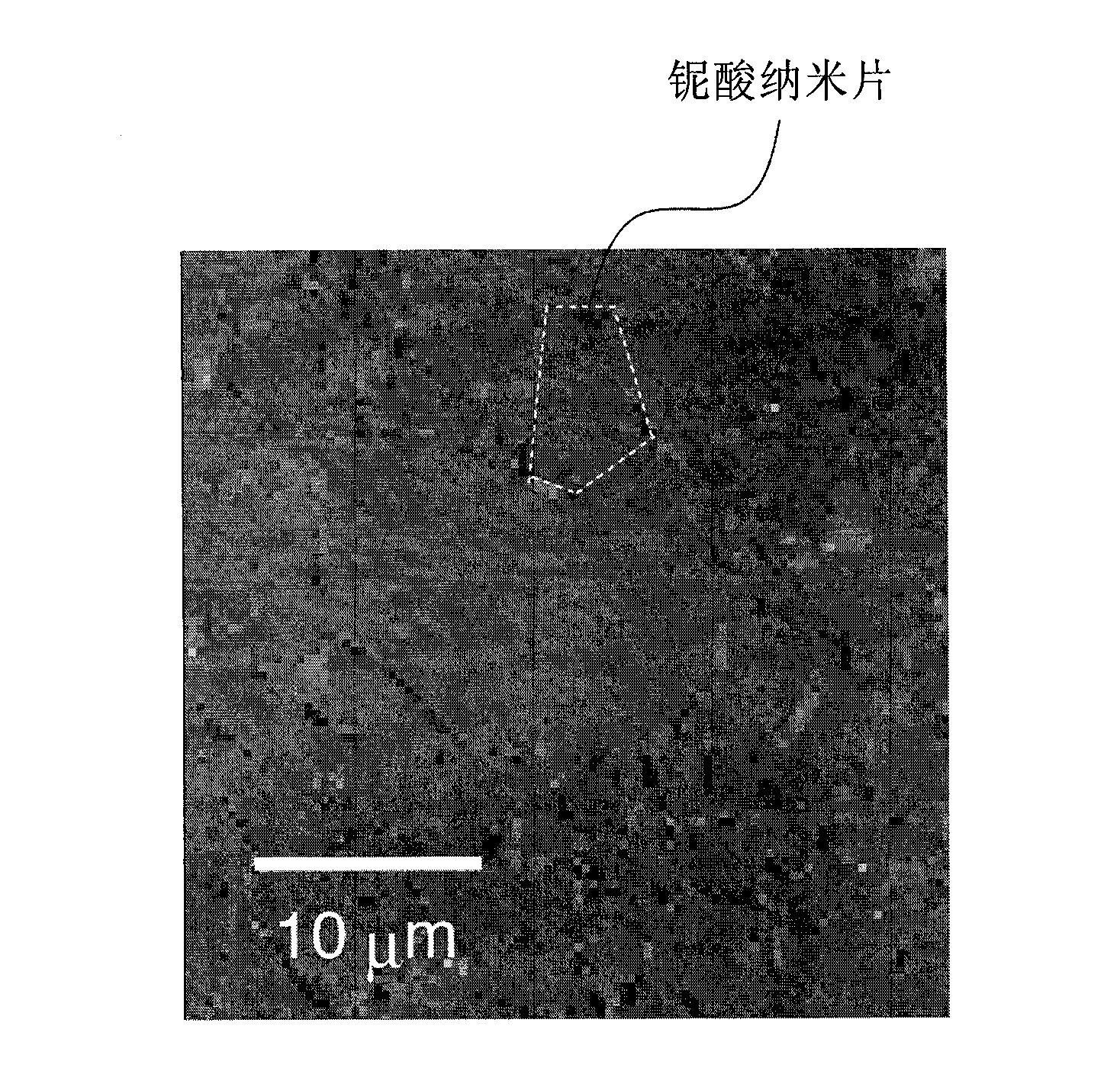
[0080] By the same method as in Example 1, the layered niobium oxide (KTiNbO 5 ) single-layer peeling, making and dispersing the composition formula TiNbO 5 It represents a milky white sol solution of rectangular nanosheets with a thickness of about 1 nm and a lateral dimension of 100 nm to 5 μm.

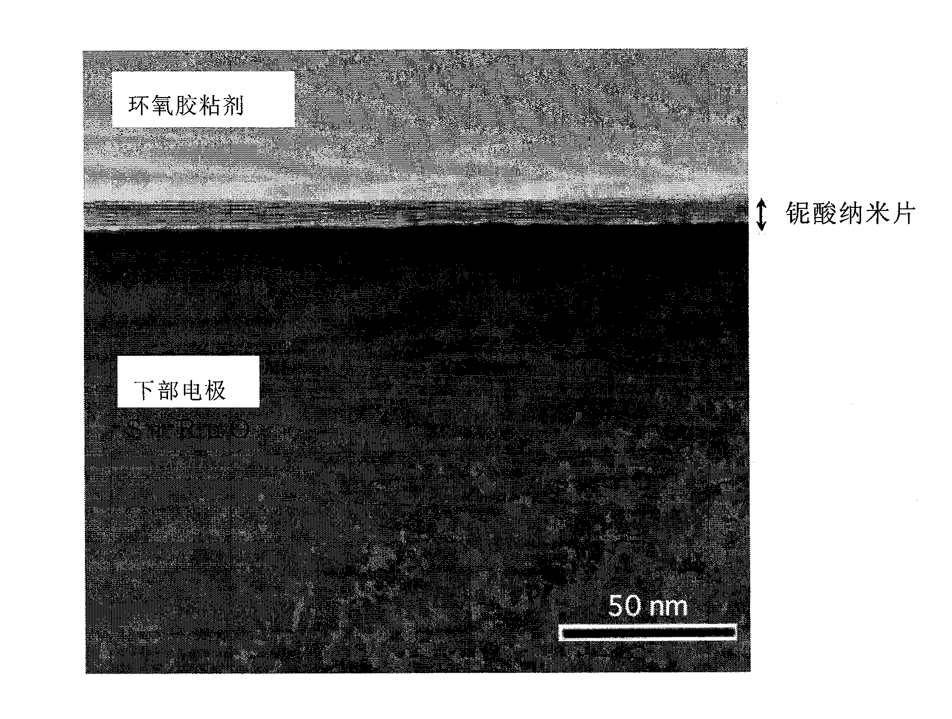
[0081] Epitaxial SrRuO by atomic planarity 3 The conductive substrate (1) of the lower electrode constituted was irradiated with ultraviolet rays under an ozone atmosphere to clean the surface, and then immersed in a solution of hydrochloric acid: methanol = 1:1 for 1 / 3 hour, and then imme...

Embodiment 3

[0092] In this embodiment, layered niobium oxide (for example, CsTi 2 NbO 7 、K 3 Ti 5 NbO 14 , KNb 3 o 8 ) as the starting material to produce niobate nanosheets (Ti 2 NbO 7 、Ti 5 NbO 14 , Nb 3 o 8 ),Such as figure 1 As shown, the atomically planar epitaxial SrRuO used as the lower electrode substrate 3 A multilayer film of the above-mentioned niobate nanosheets (2) was produced on the substrate (1) by the LB method (Langmuir-Blodgett method) as follows.

[0093] Niobate nanosheets (Ti 2 NbO 7 、Ti 5 NbO 14 , Nb 3 o 8 ) were synthesized in the following order respectively.

[0094] 2 NbO 7 Nanosheets>: cesium nitrate (CsNO 3 ), titanium oxide (TiO 2 ) and niobium oxide (Nb 2 o 5 ) were mixed in a ratio of 2.1:4:1 according to the ratio of Cs:Ti:Nb, calcined at 950°C for 1 / 2 hour, and then fired at 1100°C for 20 hours to synthesize the layered oxide CsTi 2 NbO 7 . 1 g of this powder was acid-treated in 100 mL of a prescribed hydrochloric acid aqueous s...


PUM

PropertyMeasurementUnit
thicknessaaaaaaaaaa
sizeaaaaaaaaaa
thicknessaaaaaaaaaa

Abstract

Disclosed is a dielectric film formed by attaching a single layer or a multilayer of a niobic acid nano sheet. Also disclosed is a dielectric element that can simultaneously realize a high permittivity and good insulating properties even in a nano region. The dielectric element comprises a dielectric film and other electrode disposed on the surface of the dielectric film. Further disclosed is a process for producing the dielectric element that can sweep away problems of a deterioration in a substrate interface by heat annealing in the production process, a deviation in composition from a contemplated composition caused by the deterioration in the substrate interface, and electrical mismatching, and an essential problem of a ''size effect'' that a reduction in the thickness of the film to a nano level lowers the specific permittivity and increases a leak current; can utilize unique properties and high texture and structure regulating properties possessed by the niobic acid nano sheet; and can produce the element at a low temperature free from the influence of a deterioration in substrate interface and a deviation in composition from a contemplated composition.

Description

technical field [0001] The present invention relates to a dielectric film, a dielectric element, and a dielectric film capable of achieving both a high dielectric constant and good insulating properties, which are suitable for use in a wide range of electronic materials such as DRAM memories for personal computers, multilayer capacitors for mobile phones, and gate insulators for transistors. Manufacturing method. Background technique [0002] Among dielectric components, high dielectric constant components are used in all electronic equipment such as computers and mobile phones, and play an active role in key parts of electronic equipment such as memories and transistor gate insulating films. The remarkable development of current electronic equipment such as personal computers and mobile phones depends on the high functionality of dielectric components. So far, the development and high-functionalization of dielectric elements have been achieved through micronization / integra...

Claims


Application Information

Patent Timeline
Patent Type & Authority Applications(China)
IPC IPC(8): C01G33/00H01G4/10H01G4/33H01L21/316H01L21/8242H01L27/108H01L29/78
CPCC04B2235/5454H01G4/1254C04B2235/5292C04B2235/3201C01P2004/20C01P2004/62C01G33/006H01L21/02186B82Y10/00H01L21/02175H01G4/10C04B2235/3234H01G4/30C01G35/006H01L21/31691H01L21/02194C01P2002/20H01L21/31604C04B2235/3255H01G4/33H01G4/1218C01P2004/61C04B35/495C04B35/462H01L28/40C01G33/00B82Y30/00Y10T156/10H01L21/02197H01L21/02285
Inventor 长田实佐佐木高义
Owner NAT INST FOR MATERIALS SCI
Why Eureka
Try Eureka