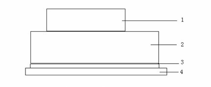
Process for cutting silicon wafer by using steel wire with diameter of 0.1mm

A steel wire and silicon wafer technology, which is applied in the process of cutting silicon wafers with a steel wire with a diameter of 0.1mm, can solve the problems of increased wire breakage rate and reduced cutting ability, and achieves reduction of cutting loss, obvious benefits, and reduced cutting loss. amount of effect

Inactive Publication Date: 2011-05-18
TIANJIN HUANOU SEMICON MATERIAL TECH CO LTD
View PDF5 Cites 24 Cited by
  • Summary
  • Abstract
  • Description
  • Claims
  • Application Information

AI Technical Summary

Problems solved by technology

[0004] Reducing the diameter of the cutting steel wire and the particle size of the cutting sand can reduce the loss of the slicing edge, but at the same time it will c

Method used


Image

  • Process for cutting silicon wafer by using steel wire with diameter of 0.1mm

Examples


Embodiment Construction

[0017] In order to understand the present invention more clearly, describe the present invention in detail in conjunction with embodiment:

[0018] The steel wire used in this example is a steel wire with a diameter of 0.10mm. The corundum is 2000# green silicon carbide, the cutting fluid is PEG205, the groove distance of the groove wheel used is 350μm, the multi-wire cutting machine model: Meyerberg DS-264; raw material: 125*125 solar square rod, the following is the used diameter 0.11 The production method and specific process of mm steel wire cutting silicon wafers:

[0019] (1) Mortar configuration: The operator will dry the corundum, the drying temperature is 40-70 degrees, and the drying time is 20-60 minutes. This example uses 40 minutes. Calculate the amount of cutting fluid and emery according to the ratio (in this example, the mass ratio of cutting fluid: emery = 1:0.95), weigh them, and prepare the mortar in the mixing bucket. The mixing time is 6-24 hours....


PUM


Abstract

The invention discloses a process for cutting a silicon wafer by using a steel wire with the diameter of 0.1mm. In the process, silicon carbide (SiC) and a cutting fluid are proportioned according to the mass ratio of 1:1 to 1:1.2; in a glue curing process, single crystals are pressurized for 0.5 to 3h by a 5 to 10kg heavy pressurizing punch to remove redundant glue; and the cutting is performed by using the steel wire with the diameter of 0.10mm under the pre-tension of 15 to 23N, a wire speed is 400 to 1,000m/min, the descending speed of a workbench is 0.3 to 1mm/min, and a cutting stroke is set according to the actual diameter of the single crystal. The process for cutting the silicon wafer by using the steel wire with the diameter of 0.1mm can effectively reduce cutting loss and improve the quality of a cut surface, achieves more remarkable benefits if the silicon wafer is thinner, and compared with the processes in which the steel wires with the diameters of 0.14mm and 0.12mm are adopted generally, saves raw materials by 6.45 percent and 2.15 percent respectively.

Description

technical field [0001] The invention relates to a process for slicing semiconductor silicon wafers, in particular to a process for cutting silicon wafers with a steel wire with a diameter of 0.1 mm. Background technique [0002] Solar cell power generation technology, with its environmental protection, inexhaustible supply, and wide range of applications, is being vigorously developed and widely used around the world. However, the current higher cost of solar cells is the biggest problem it is currently facing. [0003] Raw materials have always been the biggest cost in the processing of solar silicon wafers, reducing knife edge loss and thinning is the development direction of solar silicon wafer processing. [0004] Reducing the diameter of the cutting steel wire and the particle size of the cutting sand can reduce the loss of the slicing edge, but at the same time it will cause a decrease in the cutting ability and an increase in the wire breakage rate. When ...

Claims


Application Information

Patent Timeline
IPC IPC(8): B28D5/04
Inventor 靳立辉刘涛邢玉军郭红慧孙红永蒲福利张雪囡李翔沈浩平
Owner TIANJIN HUANOU SEMICON MATERIAL TECH CO LTD
Why Eureka
Try Eureka