Method for manufacturing medium/nitride composite structure enhanced field effect transistor

A composite structure, field effect transistor technology, applied in semiconductor/solid-state device manufacturing, electrical components, circuits, etc., can solve problems such as energy band distortion, reduce open-channel current, etc., to prevent energy band distortion, reduce series resistance, Improve the effect of 2D features

Active Publication Date: 2011-05-18
NO 55 INST CHINA ELECTRONIC SCI & TECHNOLOGYGROUP CO LTD
View PDF2 Cites 10 Cited by
  • Summary
  • Abstract
  • Description
  • Claims
  • Application Information

AI Technical Summary

Problems solved by technology

However, the channel must be pinched off with a strong negative charge, reducing the current flow in the open channel
Moreover, strong surface negative charges also cause band distortion

Method used


Image

  • Method for manufacturing medium/nitride composite structure enhanced field effect transistor
  • Method for manufacturing medium/nitride composite structure enhanced field effect transistor
  • Method for manufacturing medium/nitride composite structure enhanced field effect transistor

Examples


Embodiment 1

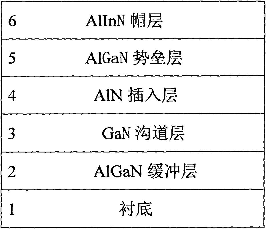
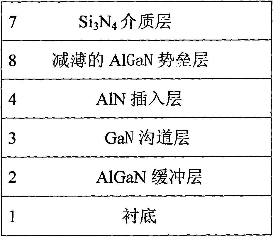
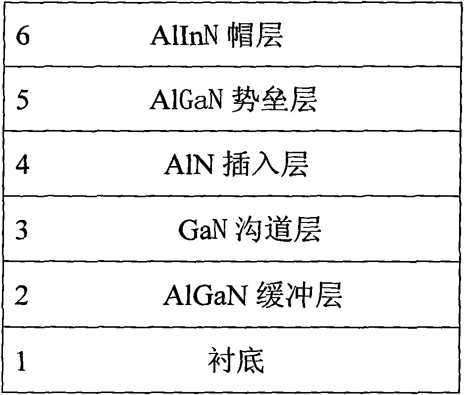
[0027] Growth of Al on substrate 1 0.04 Ga 0.96 The N buffer layer 2 and the 10nm undoped GaN channel layer 3 constitute a back barrier. Then grow a 1nm undoped AlN insertion layer 4, 5nm undoped Al on the channel layer 3 0.25 Ga 0.75 N barrier layer and 14nm undoped Al 0.83 In 0.17 The N cap layer 6 constitutes the front barrier. Calculate the band order and polarization charge on various heterogeneous interfaces, and self-consistently solve the Schrodinger equation and Poisson equation based on the effective mass and dielectric constant of each layer of material, and the electron gas density of the outer channel is calculated as 1.775*10 13 cm -2 . The electron wave function is all quantum confined in the GaN channel well, and the electron has strong two-dimensional characteristics and high transport performance. The series resistance of the outer channel and the ohmic contact resistance are reduced. Then use dry trenching process to etch the AlInN cap layer 6 and thin the A...

Embodiment 2

[0029] Growth of Al on substrate 1 0.07 Ga 0.93 The N buffer layer 2 and the 10nm undoped GaN channel layer 3 constitute a back barrier. Then grow a 1nm undoped AlN insertion layer 4, 5nm undoped Al on the channel layer 3 0.3 Ga 0.7 N barrier layer and 20nm undoped Al 0.83 In 0.17 The N cap layer 6 constitutes the front barrier. Solving the Schrodinger equation and Poisson equation in a self-consistent manner, the electron gas density of the outer channel is calculated as 1.789*10 13 cm -2 . The electron wave function is all quantum confined in the GaN channel well, and the electron has strong two-dimensional characteristics and high transport performance. The series resistance of the outer channel and the ohmic contact resistance are reduced. Then use dry trenching process to etch the AlInN cap layer 6 and thin the AlGaN barrier layer, leaving a 2nm AlGaN barrier layer, and deposit 5nm Si by ALD process 3 N 4 Layer 7, using fluorine plasma process in Si 3 N 4 Introduce 2*10 i...

Embodiment 3

[0031] Growth of Al on substrate 1 0.1 Ga 0.9 The N buffer layer 2 and the 10nm undoped GaN channel layer 3 constitute a back barrier. Then grow a 1nm undoped AlN insertion layer 4, 5nm undoped Al on the channel layer 3 0.35 Ga 0.65 N barrier layer and 25nm undoped Al 0.83 In 0.17 The N cap layer 6 constitutes the front barrier. Solving the Schrodinger equation and Poisson equation in a self-consistent manner, the electron gas density of the outer channel is calculated to be 1.738*10 13 cm -2 . The electron wave function is all quantum confined in the GaN channel well, and the electron has strong two-dimensional characteristics and high transport performance. The series resistance of the outer channel and the ohmic contact resistance are reduced. Then use dry trenching process to etch the AlInN cap layer 6 and thin the AlGaN barrier layer, leaving 2nm AlGaN barrier layer, and deposit 5nm Si by ALD process 3 N 4 Layer 7, using fluorine plasma process in Si 3 N 4 Introduce 2*10 ...


PUM


Abstract

The invention discloses a method for manufacturing a medium / nitride composite structure enhanced field effect transistor, which comprises the steps of: sequentially growing a AlGaN buffer layer, a GaN channel layer, a AlN inserting layer, a AlGaN barrier layer and a AlInN cap layer on a substrate; and forming a AlInN / AlGaN / AlN composite front barrier and a GaN / AlGaN back barrier into a high electronic air tightness external channel well limited by strong electrons. The thick AlInN cap layer with lattice match remarkably improves the electronic air tightness of an external channel, and the high and wide barriers provided by the AlInN cap layer strengthen the quantum restriction of the channel well, thus the serial resistance of the external channel is lowered and the ohmic contact resistance is reduced. After the AlInN layer is corroded by using a dry method channeling process and the AlGaN barrier layer is thinned, a Si3N4 medium layer with set thickness is deposited by using an atom layer deposition (ALD) process, thus the quantum restriction of an internal channel well is strengthened, and the ON state current of the element is improved by band distortion of a heterojunction, caused in a way that an electron wave function does not permeate into the barrier layer, under the condition that a large grid voltage change is ensured. A negative space charge is introduced on the surface of the Si3N4 medium layer by using a fluorine plasma process, thus the barrier height is increased, electron air in the internal channel well is consumed fully to ensure that the inner channel is pinched off under zero grid voltage. An ideal module enhancing work is realized.

Description

Technical field [0001] The invention relates to a method for manufacturing a semiconductor device, in particular to a method for manufacturing a dielectric / nitride composite structure enhanced field effect transistor. Specifically, the outer trench well with high density and high mobility two-dimensional electron gas is manufactured by the band tailoring method, and the trench is pinched off under zero gate voltage and opened under positive gate voltage to prevent the large positive gate voltage from being depressed. A method for manufacturing high-efficiency, high-power enhancement-mode gallium nitride field effect transistors with internal channel wells with distortion of the energy band. It belongs to the technical field of semiconductor devices. Background technique [0002] An enhanced field effect tube is a field effect tube that works under a positive grid voltage. It requires the outer channel outside the gate electrode to be opened with low series resistance, while the...

Claims


Application Information

Patent Timeline
Patent Type & Authority Applications(China)
IPC IPC(8): H01L21/335
Inventor 赵正平薛舫时石志宏
Owner NO 55 INST CHINA ELECTRONIC SCI & TECHNOLOGYGROUP CO LTD
Why Eureka
Try Eureka