

Carrier-free pin-free grid-array IC (Integrated Circuit) chip packaging part and production method thereof
A chip package and grid array technology, which is applied in the manufacture of semiconductor devices, electric solid devices, semiconductor/solid devices, etc., can solve the problems of high material cost, low pass rate, and complex frame layout structure design, and achieve heat dissipation effect Good, the design and manufacturing cycle is short, and the effect of speeding up the trial production process
- Summary
- Abstract
- Description
- Claims
- Application Information
AI Technical Summary
Problems solved by technology
Method used
Image

Examples
Embodiment 1
[0131] single chip package
[0132] 1. Thinning and scribing
[0133] Thin the wafer to 150μm first, clean it and dry it, stick the adhesive film on the back, and remove the thinning film. Then the wafer with the adhesive film attached is cut into individual chips, only the adhesive film layer is scratched, and the protective layer is not scratched.
[0134] 2. Core loading
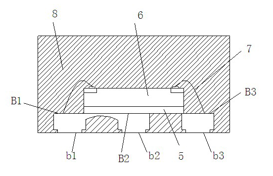
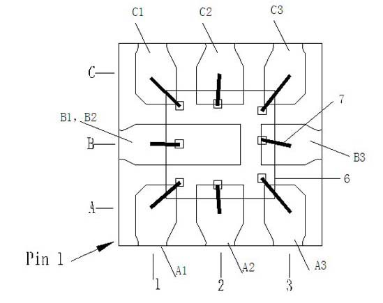
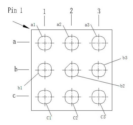
[0135] NLGA9L special frame and adhesive film are adopted. On the dedicated core loading machine, the lead frame is automatically transferred to the core loading machine track, and the chip is automatically placed on the B1, B2 inner pins and B3, A1, A2, A3, C1, C2, C3 The remaining few inner pin edges. That is, for a typical three-row pin, since the NLGA frame has no carrier, the chip with the adhesive film is glued to the B-row double pin (such as NLGA9L, B1, B2, B3) and the remaining pins (such as NLGA9L, A1 , A2, A3, C1, C2, C3), the edges are baked to achieve a firm paste.
[0136] 3. Pressure w...
Embodiment 2
[0158] Dual Die Stacked Package
[0159] The thinning, scribing, printing, and cutting of multi-chip stacked packages are the same as those of single-chip packages, and the matrix gold-plated contacts do not need electroplating.
[0160] 1. Thinning and scribing
[0161] First, the lower wafer is thinned to 200 μm, and the upper wafer is thinned to 100 μm. After cleaning and drying, the adhesive film is pasted on the back and the thinned adhesive film is removed. Then cut the wafer with the adhesive film into individual chips, adjust the scribing depth parameter according to the thickness of the thinned wafer + the film thickness of the adhesive film, and only scratch through the adhesive film layer without scratching the protective layer.
[0162] 2. Core loading
[0163] On the dedicated core loading machine for film sheets, the chip is automatically placed on the corresponding L / F inner pin setting position. After heating, the IC chip 6 is glued to the inner pins of the m...
Embodiment 3
[0186] Multi-chip package
[0187] Thinning, scribing, printing, and cutting of multi-chip packaging are the same as single-chip packaging, and the matrix lead frame uses gold-plated contacts without electroplating.
[0188] 1. Thinning and scribing
[0189] Same as Example 1
[0190] 2. Core loading
[0191] On the dedicated core loading machine for film sheets, the chip is automatically placed on the corresponding L / F inner pin setting position. After heating, the IC chip 6 is glued to the inner pins of the middle row and the edges of the remaining inner pins. For a typical four-row pin, since the NLGA frame has no carrier, the IC chip 6 with the adhesive film is glued to the B row and C row pins (such as NLGA16L: B2, B3 and C2, C3), and the adhesive film The IC chip 9 is glued to the edge of the B4 and C4 pins.
[0192] 3. Pressure welding
[0193] Since the IC chip 6 is glued to the inner pins, the pads on the IC chip are relatively close to the solder joints of the i...
PUM
 Abstract
Description
Claims
Application Information