Method for preparing metal-oxide-semiconductor field effect transistors (MOSFETs) with extremely short-gate length bulk-silicon surrounding gates

A technology of gate length and surrounding gate, which is applied in the field of microelectronic nanoscale complementary metal oxide semiconductor devices and extremely large-scale integration, can solve the problems of size reduction, large parasitic capacitance resistance, substrate pollution, etc., and achieve shortened gate length, Reduce parasitic capacitance and enhance shortening effect

Active Publication Date: 2011-06-22
SOI MICRO CO LTD
View PDF3 Cites 5 Cited by
  • Summary
  • Abstract
  • Description
  • Claims
  • Application Information

AI Technical Summary

Problems solved by technology

[0008] The main difficulty in fabricating gate-enclosed devices on bulk silicon lies in the formation of sacrificial layers. So far, there are only a few reported fabrication methods using bulk silicon substrates or damascene dummy gate processes that require complex and expensive epitaxial SiGe as a sacrificial layer. Or directly isotropically etch Si to cause contamination of the substrate, and inevitably cause large parasitic capacitance resistance, these have obvious shortcomings and limitations for further size reduction

Method used


Image

  • Method for preparing metal-oxide-semiconductor field effect transistors (MOSFETs) with extremely short-gate length bulk-silicon surrounding gates
  • Method for preparing metal-oxide-semiconductor field effect transistors (MOSFETs) with extremely short-gate length bulk-silicon surrounding gates
  • Method for preparing metal-oxide-semiconductor field effect transistors (MOSFETs) with extremely short-gate length bulk-silicon surrounding gates

Examples


Embodiment

[0075] 1) Double well process and advancement: N + The well is implanted into the Si substrate (104) using P 31+ , the energy is 110-150KeV, the dose is (1-2)e13, P + The well injected Si substrate (104) adopts B 11+ , the energy is 110-150KeV, the dose is (1-2)e13; and advance, the well depth is 1-2 microns;

[0076] 2) Isoplanar local oxidation (LOCOS) isolation, long field oxygen: 1000°C, 3000-5000 or Shallow Trench Isolation (STI);

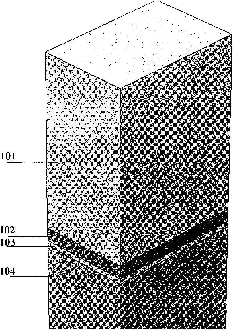
[0077] 3) As shown in Figure 1(a), CVD pads buffer SiO 2 Oxide layer (103) 15nm / SiN(102) 50nm / TEOS(101) 300nm three dielectric layers;

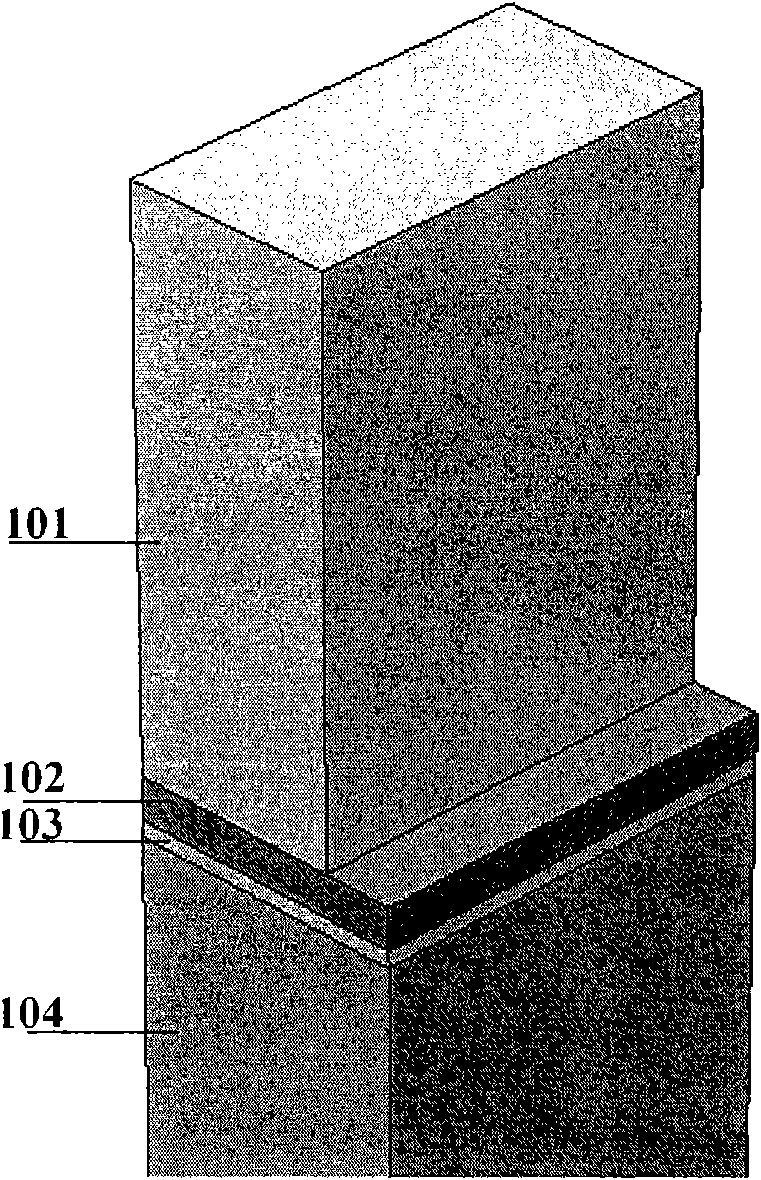
[0078] 4) As shown in Figure 1(b), a TEOS groove with a width of 120nm is etched with a positive electron beam exposure;

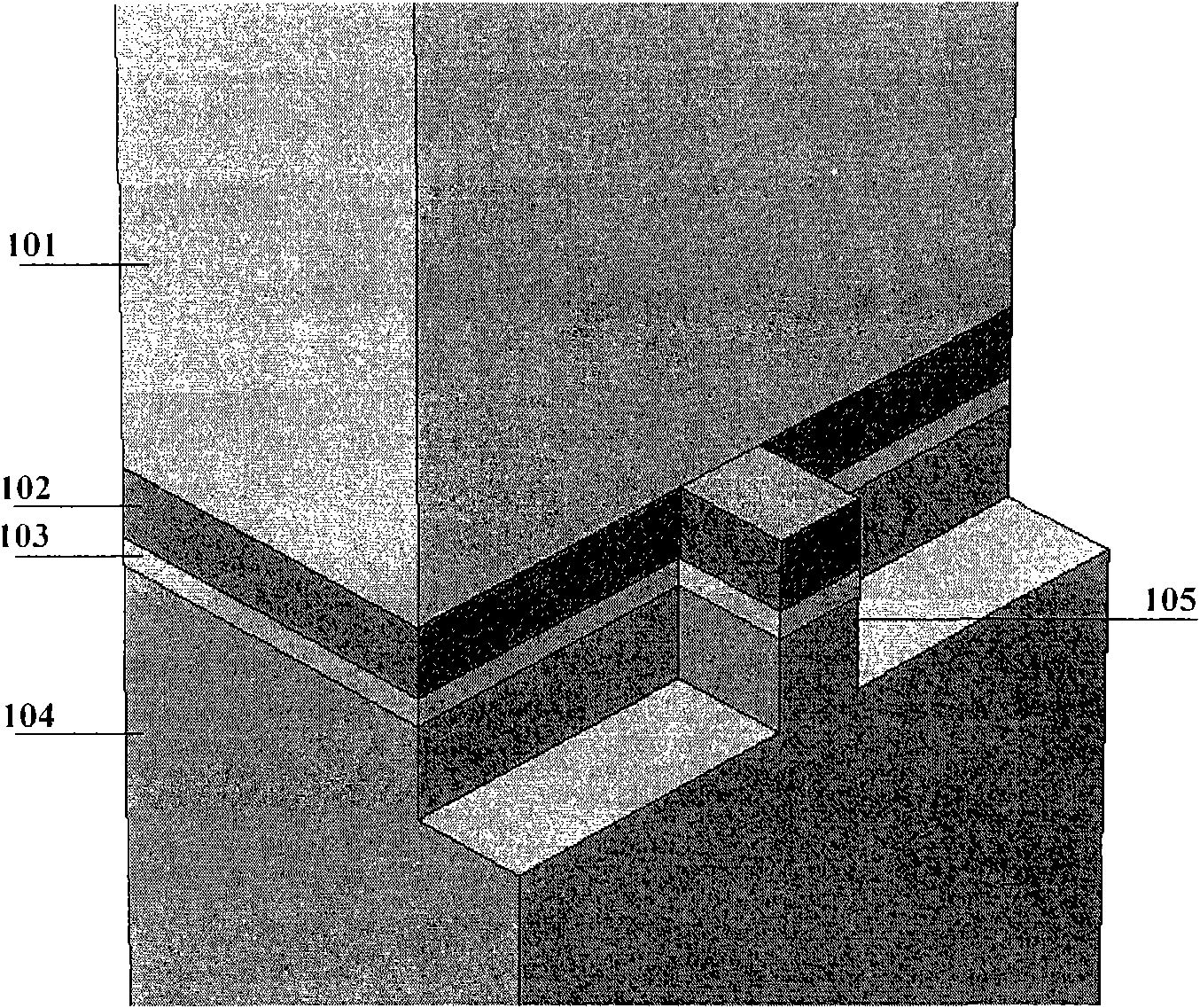
[0079] 5) As shown in Figure 1(c), use SAL601 negative electron beam exposure to etch SiN / buffered SiO in two steps in the TEOS groove 2 Oxide layer and steep fin islands (105) with a height of 100nm;

[0080] 6) As shown in Figure 1(d), build up an isotropic buffer oxide layer o...


PUM


Abstract

The invention discloses a method for preparing metal-oxide-semiconductor field effect transistors (MOSFETs) with extremely short-gate length bulk-silicon surrounding gates, which comprises the following steps of: performing local oxidation of silicon isolation or trench isolation, depositing three layers of medium films which are a cushioning SiO2 oxide layer, SiN and an oxide medium layer respectively on bulk silicon, performing electron beam exposure, etching a groove and fin, depositing SiN sidewalls, isotropically etching Si, performing dry-oxygen oxidation, performing etching to remove the sidewalls on the two sides of the fin and simultaneously reserve the bottom sidewall of the groove, performing three steps of sacrificial oxidation to form nanowires, performing wet etching to reserve sufficiently thick bottom SiO2 for isolation at the same time of releasing the nanowires, depositing a gate medium and a gate material, performing two steps of source-drain injection after the gate is back-etched, depositing and etching the sidewalls, and forming contact. The method eliminates a self-heating effect and a floating body effect, is lower in cost, well compatible with a complementary metal oxide semiconductor process by completely adopting a conventional top-down process, and favorable for inhibiting a short channel effect and promoting the development of MOSFETs with smaller sizes, and easily realizes integration.

Description

technical field [0001] The invention belongs to the technical field of microelectronic nanoscale complementary metal oxide semiconductor devices (CMOS) and extremely large-scale integration, in particular to a method for preparing metal semiconductor field-effect transistors (MOSFETs) with extremely short gate length silicon-surrounded gates . Background technique [0002] Nano-CMOS devices continue to develop in accordance with Moore's law, and the continuous reduction of the size of planar bulk silicon devices has encountered severe challenges. Various new structure devices have emerged, and the gate structure of the device has evolved from the initial single gate to double gate and triple gate. From the surrounding gate structure that completely surrounds the channel, the gate control ability and the ability to suppress the short channel effect are continuously enhanced with the increase in the number of gates. The nanowire-enclosed gate MOSFET with surrounding channel s...

Claims


Application Information

Patent Timeline
Patent Type & Authority Applications(China)
IPC IPC(8): H01L21/336H01L21/28
Inventor 宋毅徐秋霞周华杰
Owner SOI MICRO CO LTD
Why Eureka
Try Eureka