Preparation method of silicon-based nano-wire solar cell
A solar cell and silicon-based nanotechnology, applied in the manufacture of circuits, electrical components, and final products, can solve problems such as high surface recombination rate, poor electrode contact, and low efficiency of nanowire batteries
- Summary
- Abstract
- Description
- Claims
- Application Information
AI Technical Summary
Problems solved by technology
Method used
Image
Examples
example 1
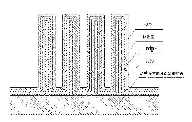
[0037] 1. AZO / nano-silicon nip / Al 2 o 3 / AZO radial structure nanowire solar cell structure see figure 1 .
[0038] 2. Preparation of solar cells
[0039] 1. Preparation of AZO nanowire arrays:
[0040] (1) ITO glass substrate is selected, and the square resistance is 10 Ω;
[0041]Zinc acetate and citric acid were mixed at a molar ratio of 1:1, anhydrous ethanol was used as a solvent, and a 0.4 M ZnO transparent homogeneous sol was prepared by ultrasonic dissolution, which was aged for 2 days and coated on the substrate by spin coating. Annealing in the annealing furnace, annealing conditions: 350 o C, 10 min; repeat this process 10 times, then put it into the heating furnace, at 550 o C for 2 h to prepare a zinc oxide (ZnO) seed layer.
[0042] (2) Using zinc nitrate, aluminum nitrate, diethylenetriamine and water, ultrasonically dissolved to prepare a 0.004 M precursor solution, the molar ratio of Al and Zn in the precursor solution was 2.5%; soak the above substrate...
example 2
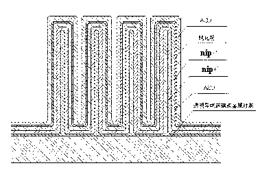
[0059] 1. AZO nanowire / nano-silicon nip / nano-silicon nip / Al 2 o 3 / AZO transparent upper electrode radial structure nanowire solar cell structure see figure 2 .
[0060] 2. Preparation of solar cells
[0061] 1. Preparation of AZO nanowire arrays:
[0062] Same as 1 in Example 1.
[0063] 2. Use PECVD to grow a 5nm thick n-type nano-silicon layer:
[0064] Same as 2 in Example 1.
[0065] 3. Use PECVD to grow a 20 nm thick intrinsic nano-silicon layer:
[0066] Growth conditions: silane with hydrogen dilution ratio of 95%, growth temperature 300°C, silane flow rate 10 sccm, hydrogen
[0067] Flow rate 100sccm, RF power 80W.
[0068] 4. Use PECVD to grow a p-type nano-silicon layer with a thickness of 5nm:
[0069] Same as 4 in Example 1.
[0070] 5. Using PECVD to grow n-type nano-silicon with a thickness of 5nm
[0071] Growth conditions: Silane at a hydrogen dilution ratio of 95%, the dilution ratio of borane [PH 3 ] / [PH 3 + H 2 ] is 0.5%, the g...
PUM
| Property | Measurement | Unit |
|---|---|---|
| diameter | aaaaa | aaaaa |
| length | aaaaa | aaaaa |
| thickness | aaaaa | aaaaa |
Abstract
Description
Claims
Application Information

