

Metal nanocrystalline storage capacitor and preparation method thereof
A metal nanocrystal, storage capacitor technology, applied in semiconductor/solid-state device manufacturing, circuits, electrical components, etc., can solve problems such as difficult adjustment, reduce energy consumption and cost, achieve good uniformity, and achieve the effect of complete isolation
- Summary
- Abstract
- Description
- Claims
- Application Information
AI Technical Summary
Problems solved by technology
Method used
Image

Examples
Embodiment 1
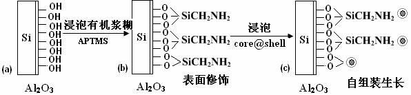
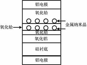
[0037] figure 2 It is a schematic diagram of the self-assembly process of core@shell bimetallic nanocrystals on alumina media. Among them, the aluminum oxide medium adopts the method of atomic layer deposition, and the thickness is 5-7 nanometers, and the bimetallic nanocrystal with core@shell structure is prepared by one-step reduction method. image 3 is a schematic cross-sectional view of the prepared double-layer metal nanocrystal storage capacitor. The preparation process of the storage capacitor is as follows:
[0038] 1. After the standard cleaning of the p-type silicon wafer, then atomic layer deposition of Al with a thickness of 3 to 4 nanometers is sequentially deposited on the silicon wafer. 2 o 3 Dielectric and HfO with a thickness of 1~2nm 2 dielectric, this stack acts as a tunneling layer. Atomic Layer Deposition Al 2 o 3 The reaction precursors of the medium are trimethylaluminum (TMA) and water; the deposition temperature is controlled at 280-320 °C. ...
Embodiment 2
[0046] Prepare bimetallic nanocrystal sol solution by one-step reduction method: 1354 microliters of sodium tetrachloropalladate solution with a concentration of 0.05 mol / microliter, 152 microliters of 0.05 moles / microliter of potassium chloroplatinite solution and 753 microliters EDTA (0.1 mol / µl) was added to 26 ml of water. The mixed solution was stirred vigorously for 40 minutes, and the temperature of the system was maintained at 60 °C. Wait for the mixed solution to cool to room temperature, add 6 ml of a mixed solution containing 0.05 mol of sodium carbonate and 18 mg of sodium borohydride dropwise, and the dosage is controlled at a rate of 0.3 ml per minute by a peristaltic pump. Stirring was continued at room temperature for 2 hours, and then the suspension was filtered, rinsed with a large amount of deionized water, and dried overnight at 70°C in a vacuum environment. Figure 4 is the Pd prepared by this method 0.9 Pt 0.1 TEM image of bimetallic nanocrystals. It ...
Embodiment 3
[0048] Trimetallic nanocrystal sol solution prepared by seed-mediated epitaxial growth method: 6 ml of 10 mmol sodium borohydride solution was added dropwise to 44 ml of silver nitrate (1.0 mmol) and sodium citrate (1.0 mmol) in solution. Stir vigorously at 0°C for three hours to obtain a silver sol with a size of 7 nm.
[0049] A solution of sodium tetrachloropalladate and potassium chloroplatinite with a total ion content of 0.04 mmol was dissolved in 20 ml of water and then sonicated for 60 minutes. Heat the mixed solution to boil. After boiling for 10 minutes, 30 milliliters of the previously prepared silver sol was added dropwise. Stirring was continued for 2 hours under heating, the suspension was filtered out, washed with a large amount of hot water, and dried overnight at 70°C in a vacuum environment. Figure 5 It is a TEM photo of the obtained hollow ternary metal nanocrystal. It can be seen that the diameter of the hollow is about 3 nanometers, and the diameter of...
PUM
| Property | Measurement | Unit |
|---|---|---|
| Thickness | aaaaa | aaaaa |
| Thickness | aaaaa | aaaaa |
| Thickness | aaaaa | aaaaa |
Abstract
Description
Claims
Application Information