

Multilayer copper interconnection manufacturing method
A manufacturing method and copper interconnection technology, applied in semiconductor/solid-state device manufacturing, electrical components, circuits, etc., can solve problems such as inability to use plasma, many technical processes, and complicated processes
- Summary
- Abstract
- Description
- Claims
- Application Information
AI Technical Summary
Problems solved by technology
Method used
Image

Examples
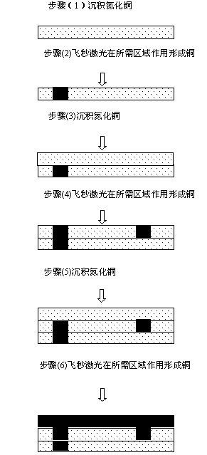
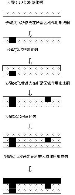
example 1
[0017] 1. Deposit copper nitride on the silicon wafer by sputtering method;
[0018] On the silicon wafer, copper nitride is deposited by sputtering. The sputtering target adopts pure copper target (99.999%), and the background vacuum is 1.0×10 -4 Pa, substrate temperature 150 o C, the working gas is high-purity nitrogen (99.999%), the gas flow rate is controlled at 30 sccm, the working pressure is controlled at about 1Pa, and copper nitride with a thickness of 100 nanometers is deposited.
[0019] 2. Use femtosecond laser to position and heat the required area to decompose copper nitride into copper;
[0020] The specific parameters of the femtosecond laser incident on the copper nitride film are: wavelength 200 nm, pulse width 25 femtoseconds, pulse energy 0.5 mJ, repetition rate 1000 Hz;
[0021] Adjust the height of the sample stage so that the femtosecond laser is focused on the surface of the copper nitride film, and the sample stage moves horizontally at a speed of 0...
PUM
| Property | Measurement | Unit |
|---|---|---|
| thickness | aaaaa | aaaaa |
| wavelength | aaaaa | aaaaa |
Abstract
Description
Claims
Application Information