

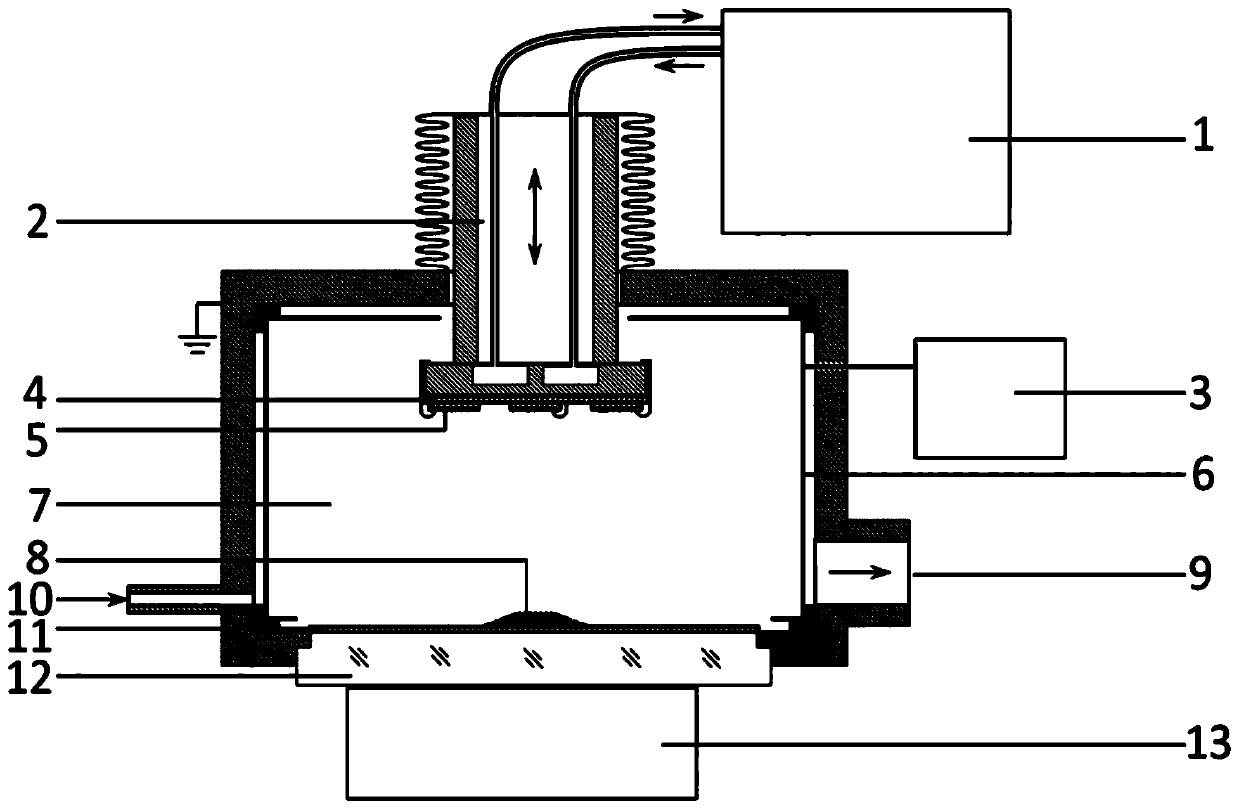
A plasma activated doping device
A plasma and semiconductor technology, applied in the field of semiconductor doping, can solve the problems of inability to meet the requirements of bombardment intensity, failure to achieve doping purposes, contamination of semiconductor samples, etc., and achieve short doping treatment time and no etching effect. , the effect of reducing contamination
- Summary
- Abstract
- Description
- Claims
- Application Information
AI Technical Summary
Problems solved by technology
Method used
Image

Examples
Embodiment 1
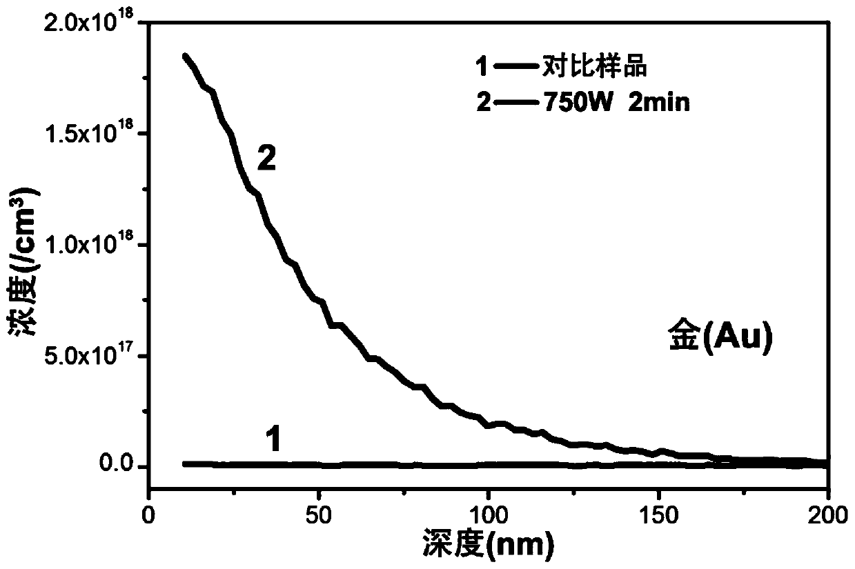
[0027] Embodiment 1: Au-doped Si semiconductor wafer at room temperature
[0028] The surface of the doped semiconductor table 2 is covered with a Si wafer (semiconductor wafer 4 for masking) and fixed with a tungsten needle, and the 10mm×10mm doped Si sample is also fixed on the surface of the Si wafer for masking with a tungsten needle, and is held by the doped semiconductor table 2. At room temperature, the distance from the plasma source is 150 mm. The surface of the plasma coupling window 12 is covered with a Si high-resistance sheet (impurity source platform 11 ) of the same diameter, on which Au foil is placed as a dopant source. The vacuum chamber 7 was filled with He gas, the flow rate was 22 sccm, the pressure was controlled between 3E-2Pa and 6E-2Pa, the output power of the excitation RF power supply of the plasma generation unit was set to 750W, and the duration of diffusion doping was 2min. figure 2 The impurity Au concentration distribution along the depth dire...
Embodiment 2
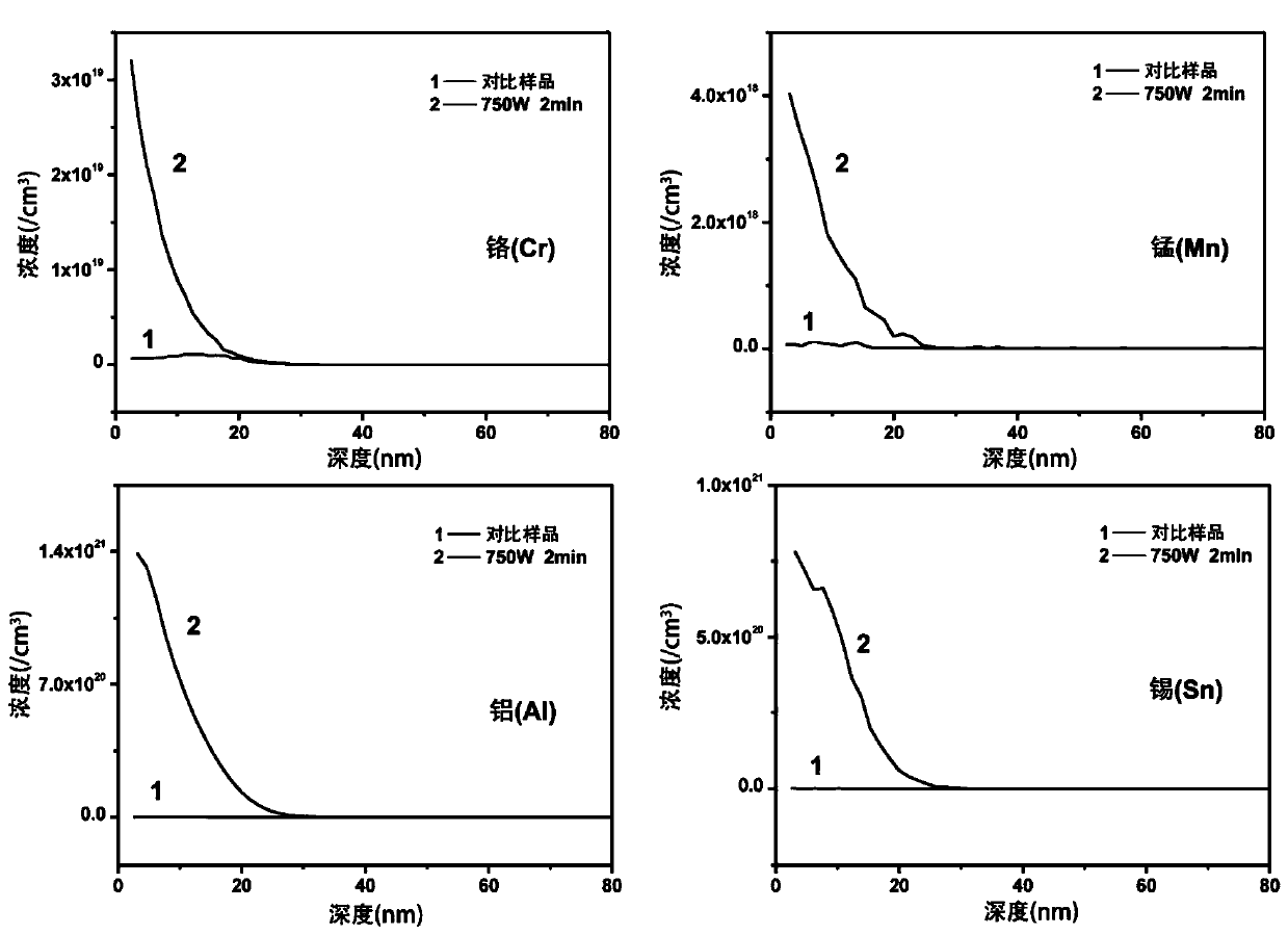
[0029] Embodiment 2: room temperature GaAs semiconductor wafer doped with Cr, Mn, Al and Sn
[0030] The surface of the doped semiconductor table 2 is covered with a GaAs wafer (semiconductor wafer 4 for masking) and fixed with tungsten needles, and the 10mm×10mm doped n-type GaAs sample is also fixed on the surface of the covered GaAs wafer with tungsten needles, and the plasma coupling window The surface of 12 is covered with a GaAs high-resistance sheet (impurity source platform 11) with the same diameter and size, on which flaky or granular Cr, Mn, Al and Sn are placed as doping sources. Other doping conditions are the same as Example 1. image 3 The impurity concentration distribution along the depth direction of GaAs sheet doped with Cr, Mn, Al and Sn measured by secondary ion mass spectrometry. The diffusion depth of Cr, Mn, Al and Sn is about 20nm, and the diffusion coefficients obtained by fitting the residual error function are 2.3E-15, 3.0E-15, 4.3E-15 and 3.7E-15c...
Embodiment 3
[0031] Embodiment 3: Room temperature GaN semiconductor wafer doped with Si, Mg and Ca
[0032] The surface of the doped semiconductor table 2 is covered on the GaN wafer grown by MOCVD on the sapphire substrate (semiconductor wafer 4 for masking), fixed with tungsten needles, and the doped GaN sample is also fixed on the surface of the GaN wafer for covering with tungsten needles, The surface of the plasma coupling window 12 is covered with a GaN wafer (impurity source platform 11) also grown by MOCVD on the sapphire substrate, the diameter of which is the same as that of the plasma coupling window 12, and Si wafers, Mg and Ca particles are placed on it as dopant sources. Other doping experimental conditions are the same as in Example 1. Figure 4 The impurity concentration distribution along the depth direction of GaN flake doped with Si, Mg and Ca measured by secondary ion mass spectrometry. The diffusion depths of Si, Mg, and Ca are 20, 10, and 7 nm, respectively, and the...
PUM
 Abstract
Description
Claims
Application Information