Device and method for manufacturing micro-nano structure

A technology of micro-nano structure and manufacturing device, applied in the fields of nano-structure manufacturing, nanotechnology, nanotechnology, etc., can solve the problems of complex operation, expensive equipment, limited processing accuracy, etc.

Inactive Publication Date: 2011-10-05
BEIJING UNIV OF CHEM TECH
View PDF5 Cites 13 Cited by
  • Summary
  • Abstract
  • Description
  • Claims
  • Application Information

AI Technical Summary

Problems solved by technology

Among them, except two-photon processing technology, rapid prototyping technology (RPM) and micro-machining technology of ultra-precision micro-machine tools, other technologies can only be used for two-dimensional or quasi-three-dimensional microstructure processing, but they all have poor ability to accurately control the longitudinal processing scale. problems; the equipment used in two-photon processing technology is expensive, the operation is complicated, and the processing accuracy is limited. In the application of micro-nano structure processing, further research is needed; RPM has certain restrictions on the materials used, and it uses energy beam processing. However, although the micromachining technology of micro-high-precision ultra-precision machine tools is not limited by materials, it is limited by the manufacturing accuracy of machine tools and the size and accuracy of tools. In terms of the size of parts for processing three-dimensional structures, it is still on the order of microns to sub-microns, and cannot reach the order of nanometers

Method used


Image

  • Device and method for manufacturing micro-nano structure
  • Device and method for manufacturing micro-nano structure
  • Device and method for manufacturing micro-nano structure

Examples


Embodiment Construction

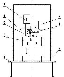
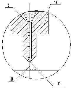
[0024] A micro-nano structure manufacturing device of the present invention, such as Figure 1~2 The schematic diagram shown mainly includes a ball pen 1, a plating solution 2, a ball pen stand 3, an atomic force microscopic detection system 4, a cathode platform 5, a micro-motion workbench 6, and a micro-electric power supply 7, in which the ball pen containing the plating solution 1 is fixed on the atomic pen stand 3 to support the atomic pen 1, the atomic pen stand 3 is integrated with the atomic force microscopic detection system 4, and the rough positioning and precise positioning are performed on it, and the cathode platform 5 is fixedly connected to the micro-motion workbench 6 , separated by insulating material between the cathode platform 5 and the micro-movement workbench 6, the ball pen refill 10 is connected with the positive pole of the micro-electric power supply 7, and the cathode platform 5 is connected with the negative pole of the micro-electric power supply 7...


PUM


Abstract

The invention discloses a device and method for manufacturing a micro-nano structure, belonging to the field of micro-nano manufacture. The device mainly comprises a ballpoint pen, a plating solution, a ballpoint pen rack, an atomic force micro detection system, a cathode platform, a micro motion workbench and a trace electricity power supply, wherein the ballpoint pen containing the plating solution is fixed on the ballpoint pen rack, the ballpoint pen rack is integrally connected with the atomic force micro detection system and is used for roughly positioning and accurately positioning the atomic force micro detection system, the cathode platform and the micro motion workbench are fixedly connected and are spaced by using an insulation material, a ballpoint pen refill is connected with the anode of the trace electricity power supply, and the cathode platform is connected with the cathode of the trace electricity power supply. In the invention, by the application of the trace electricity power supply and a carbon nanotube, atomic assembly, atomic group sedimentation and three-dimensional micro-nano molding become easier, simpler and more precise. The device and the corresponding molding method have certain significances to precise manufacture of micro-nano devices, micro-nano electromechanical progress and development of quantum devices.

Description

technical field [0001] The invention relates to a micro-nano product molding device and a molding method thereof, belonging to the field of micro-nano device molding. Background technique [0002] With the development of nanotechnology, the demand for micro-nano systems, micro-nano scale parts and related products [0003] more and more. Whether it is the processing of Micro Electro Mechanical System (MEMS) parts or the construction of micro-nano functional structures, it is inseparable from the manufacturing and processing technology of micro-nano structures. With the continuous breakthrough of cutting-edge technologies, new processing methods are constantly emerging. Generation and improvement, extreme manufacturing technology must become the key development direction of modern processing technology. [0004] At present, the microstructure processing technology mainly includes LIGA technology, three-beam (electron beam, ion beam, photon beam) micromachining technology, m...

Claims


Application Information

Patent Timeline
Patent Type & Authority Applications(China)
IPC IPC(8): B82B3/00B82Y40/00
Inventor 杨卫民李好义丁玉梅
Owner BEIJING UNIV OF CHEM TECH
Why Eureka
Try Eureka