Method, optical mask and photoreaction layer for making substrate of color filter

A color filter and manufacturing method technology, applied in the direction of filter, optics, optical components, etc., can solve the problems of inconsistent height and pixel ActiveArea area, complicated process, light leakage, etc., to improve contrast and light transmittance, The effect of shortening cycle times and simplifying process steps

Inactive Publication Date: 2011-10-12
TCL CHINA STAR OPTOELECTRONICS TECH CO LTD
View PDF2 Cites 22 Cited by
  • Summary
  • Abstract
  • Description
  • Claims
  • Application Information

AI Technical Summary

Problems solved by technology

[0004] The current manufacturing methods of color filter substrates mostly use BM / R / G / B / ITO / PS as the manufacturing process, and the color separation effect cannot be achieved by one exposure, so coating and exposure must be carried out in stages and developing steps to form different color resist layers; it is also limited by this, so it is necessary to open different masks (Mask) according to the accuracy of the machine, and perform alignment exposure on different machines. Accuracy problems will lead to a decrease in the aperture ratio during design
In addition, because it needs to be produced in multiple layers, the height of the area where the R / G / B layer is stacked on the BM will be inconsistent with the pixel Active Area area (hereinafter referred to as the AA area), resulting in different liquid crystal tilt angles and light leakage. reduce contrast
[0005] Therefore, the current manufacturing method of the color filter substrate has the defects that the manufacturing process is complicated and it is easy to cause the decrease of the aperture ratio and the decrease of the display contrast.

Method used


Image

  • Method, optical mask and photoreaction layer for making substrate of color filter
  • Method, optical mask and photoreaction layer for making substrate of color filter
  • Method, optical mask and photoreaction layer for making substrate of color filter

Examples


specific Embodiment approach

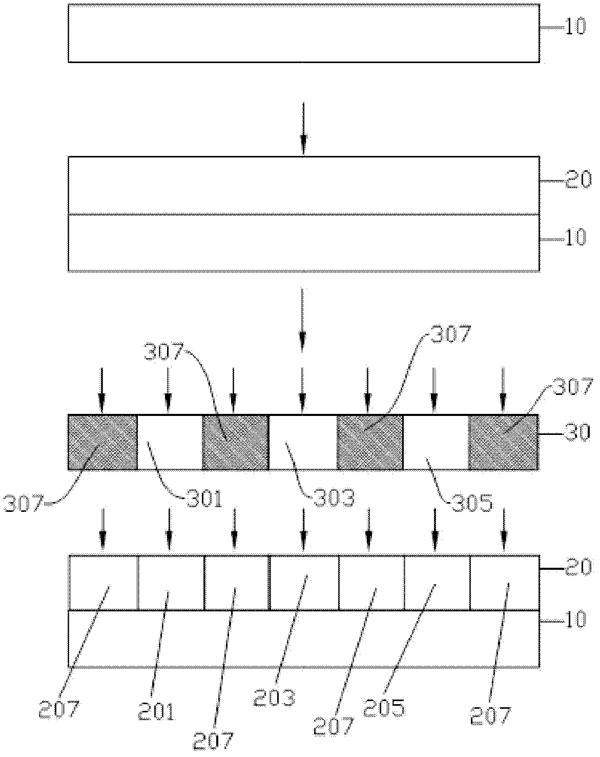
[0069] In addition, the present invention also has other specific implementation modes, for example: the first frequency band light transmission area 301, the second frequency band light transmission area 303 and the third frequency band light transmission area 305 are correspondingly set in the first light transmission area of ​​the optical mask 30 A laser diode with a single wavelength that emits light in the first frequency band, light in the second frequency band, and light in the third frequency band is used as a light source to irradiate the photoreactive layer 20; The single-wavelength laser diodes of the light of the first frequency band, the light of the second frequency band and the light of the third frequency band are used as light sources to irradiate the second light-transmitting region 307 .

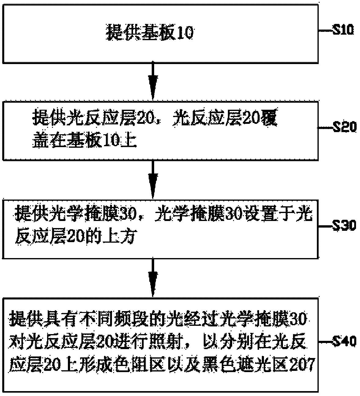
[0070] Different from the prior art, the present invention covers the photoreactive layer 20 on the substrate 10, and arranges the optical mask 30 above the photoreactive l...


PUM


Abstract

The invention discloses a method, an optical mask and a photoreaction layer for making a substrate of a color filter. The method comprises the following steps of: providing the substrate; providing the photoreaction layer, wherein the photoreaction layer is coated on the substrate; providing the optical mask, wherein the optical mask is arranged above the photoreaction layer; and providing light of different frequency ranges to irradiate the photoreaction layer through the optical mask so as to respectively form a color resistance area and a black shading area on the photoreaction layer. The invention also provides the optical mask and the photoreaction layer for making a color resistance layer of the substrate of the color filter. By adopting the mode, the method has the advantages of shortening the cycle period of processing and improving the aperture opening ratio and the display contrast ratio.

Description

technical field [0001] The invention relates to the field of liquid crystal display, in particular to a manufacturing method of a color filter substrate, an optical mask and a photoreactive layer. Background technique [0002] Liquid Crystal Display (LCD) not only has the characteristics of being light, thin, and small, but also has the advantages of low power consumption, no radiation, and relatively low manufacturing cost, so it currently occupies a dominant position in the field of flat panel display. Liquid crystal displays are ideally suited for use in desktop computers, palmtop computers, personal digital assistants (Personal Digital Assistant, PDA), cellular phones, televisions, and a variety of office automation and audio-visual equipment. [0003] The liquid crystal display panel is the main component of the liquid crystal display device. At present, the mainstream liquid crystal display panel is composed of a thin-film transistor (Thin-film transistor, TFT) substra...

Claims


Application Information

Patent Timeline
Patent Type & Authority Applications(China)
IPC IPC(8): G02B5/20G03F1/14G02F1/1335
CPCG02B5/201G02B5/22G02F1/133516
Inventor 陈孝贤李冠政
Owner TCL CHINA STAR OPTOELECTRONICS TECH CO LTD
Why Eureka
Try Eureka