Silver nano superstructure array, and preparation method and application thereof

A superstructure and silver nanotechnology, which is applied in the field of chemical materials, can solve the problems of poor effective specific structure control and poor order control, and achieve the effect of enhancing photoelectric conversion efficiency and high positioning accuracy

Inactive Publication Date: 2011-11-09
THE NAT CENT FOR NANOSCI & TECH NCNST OF CHINA
View PDF5 Cites 17 Cited by
  • Summary
  • Abstract
  • Description
  • Claims
  • Application Information

AI Technical Summary

Problems solved by technology

The former has precise surface positioning accuracy and complex surface patterning capabilities on a large scale, but has poor control over the effective specific structure on a small scale; the latter can be effectively specific on a small scale as needed Structure control, and easy to achieve large-scale low-cost preparation, but poor in large-scale order control

Method used


Image

  • Silver nano superstructure array, and preparation method and application thereof
  • Silver nano superstructure array, and preparation method and application thereof
  • Silver nano superstructure array, and preparation method and application thereof

Examples


Embodiment 1

[0064] The silicon wafers in this embodiment were purchased from Beijing Zhongjing Keyi Technology Co., Ltd., the product name is monocrystalline silicon wafer, and the product number is P556359.

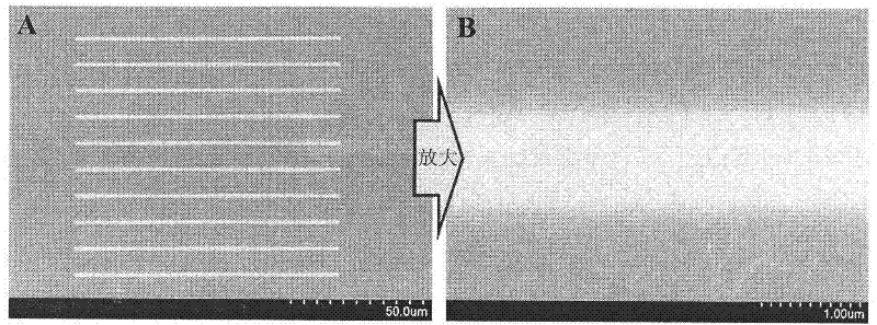
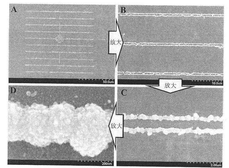
[0065] Silver nano-superstructure arrays on silicon wafer surface composed of one-dimensional necklace-like silver nano-superstructure lines preparation.

[0066] (1) Cut the commercial polished silicon wafer of P type 4 into small pieces of 1.5cm×1.5cm with a dicing machine.

[0067] (2) The cut silicon wafers were ultrasonically cleaned with acetone, ethanol and secondary water for 5 minutes in sequence, and then blown dry with nitrogen after removing surface pollutants.

[0068] (3) Glue the clean silicon wafers sequentially in the ultra-clean room according to the pre-designed line array pattern (the coating material is polymethyl methacrylate, and the coating amount is 1-2 μm thick). The silicon wafer is exposed under the SEM electron beam. During the exposure, the compute...

Embodiment 2

[0077] Fabrication of silver nanosuperstructure arrays on silicon wafer surface composed of one-dimensional rod-like silver nanosuperwires.

[0078] Step (1)-(8) is the same as embodiment 1

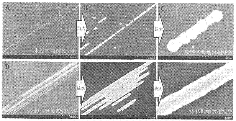
[0079] (9) immerse the patterned silicon wafer pretreated by electron beam exposure and reactive ion beam etching in hydrofluoric acid with a volume concentration of 40% for 1 hour and then immerse in the silver ion-cysteine ​​complex solution, Then put them into a 37°C electric incubator and cultivate them for 2 days.

[0080] (10) Take out the cultured silicon chip, wash it repeatedly with secondary water to remove the residual solution on the surface, and then blow it dry with nitrogen to obtain a silver nano-superstructure array on the surface of the silicon chip composed of one-dimensional rod-shaped silver nano-superstructure lines.

[0081] Example 1 Steps (1)-(4) The surface of the silicon wafer after electron beam exposure and reactive ion beam etching surface patterning pretr...

Embodiment 3

[0083] SERS detection

[0084] (1) p-aminothiophenol (abbreviated as PATP in English) is dissolved in the mixed solvent of methanol and water with a volume ratio of 1:1 to form a concentration of 10 -10 M's solution.

[0085] (2) Dilute 100μL concentration to 10 -10 The PATP solution of M is added in the specially-made SERS sample groove, then the silicon wafer with the silver nanometer superstructure array that embodiment 1 prepares is immersed, carries out SERS signal collection (laser 633nm; Power about 2mW; Exposure time 10s), the result shows that this The PATP detection limit of silver nano-superstructure array on the surface of a silicon wafer can reach 10 -10 M.


PUM

PropertyMeasurementUnit
widthaaaaaaaaaa
diameteraaaaaaaaaa
diameteraaaaaaaaaa

Abstract

The invention provides a silver nano superstructure array. The silver nano superstructure array is arranged on the surface of a substrate. The invention also provides a preparation method for the silver nano superstructure array. The preparation method comprises the following steps of: putting a patterned silicon wafer into a silver ion-cysteine complexing solution with the pH value of 10.0 to 11.0; and culturing the patterned silicon wafer at the temperature of between 4 and 45 DEG C for 1 to 3 days to obtain the silver nano superstructure array. The invention further provides application ofthe silver nano superstructure array to surface enhanced Raman spectrum (SERS) detection and solar batteries. The silver nano superstructure array prepared by the method has high sensitivity and highly uniform SERS detection effect.

Description

technical field [0001] The invention relates to a silver nano superstructure array, a preparation method and application of the silver nano superstructure array, and belongs to the field of chemical materials. Background technique [0002] The compounds adsorbed on the roughened metal surface are electromagnetically enhanced (that is, physically enhanced) due to the excitation of surface localized plasmons, and the atomic clusters on the rough surface and the molecules adsorbed on it constitute the Raman-enhanced active sites ( That is: chemical enhancement), the effect of the two makes the measured Raman scattering produce a great enhancement effect, and its enhancement factor can reach 10 3 -10 7 . It has been found that the metals that can produce surface-enhanced Raman spectroscopy (SERS) include Ag, Au, Cu, and Pt, among which Ag has the best enhancement effect. This technique has the advantages of good selectivity and high sensitivity, and the actual detection limit...

Claims


Application Information

Patent Timeline
Patent Type & Authority Applications(China)
IPC IPC(8): B22F1/00B22F9/24
Inventor 李超唐智勇
Owner THE NAT CENT FOR NANOSCI & TECH NCNST OF CHINA
Why Eureka
Try Eureka