Ultraviolet avalanche photodetector with PIN inverted structure and preparation method thereof

A photodetector and ultraviolet avalanche technology, applied in the field of ultraviolet detectors, can solve the problems of complex process, difficult testing, large lattice and thermal mismatch, etc., to simplify the process, reduce the difficulty of testing, and improve the detection sensitivity. Effect

Inactive Publication Date: 2011-11-16
SUN YAT SEN UNIV
View PDF4 Cites 18 Cited by
  • Summary
  • Abstract
  • Description
  • Claims
  • Application Information

AI Technical Summary

Problems solved by technology

[0009] (1) In order to obtain good performance, when using back-incidence, substrate thinning and double-sided polishing are required, and the process is complicated;
[0010] (2) When using the probe station to test the device performance, when the optical signal adopts the back-incidence method, it is not easy to test
[0011] (3) In the traditional structure, the optical signal will be absorbed and scattered when it enters the p-type layer from the substrate and buffer layer through the back-incidence method, which will reduce the external quantum efficiency of the detector; if the buffer layer uses an AlGaN buffer layer, it will Because the lattice and thermal mismatch between the AlGaN buffer layer and the substrate material is larger than that of the GaN buffer layer, high-density defects are generated in the AlGaN buffer layer and the active layer grown on it, which deteriorates the key performance of the device, such as dark current, quantum efficiency, etc.

Method used


Image

  • Ultraviolet avalanche photodetector with PIN inverted structure and preparation method thereof
  • Ultraviolet avalanche photodetector with PIN inverted structure and preparation method thereof
  • Ultraviolet avalanche photodetector with PIN inverted structure and preparation method thereof

Examples


Embodiment Construction

[0034] The present invention will be described in detail below with reference to the accompanying drawings.

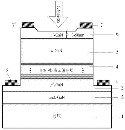
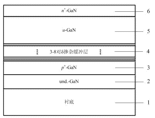
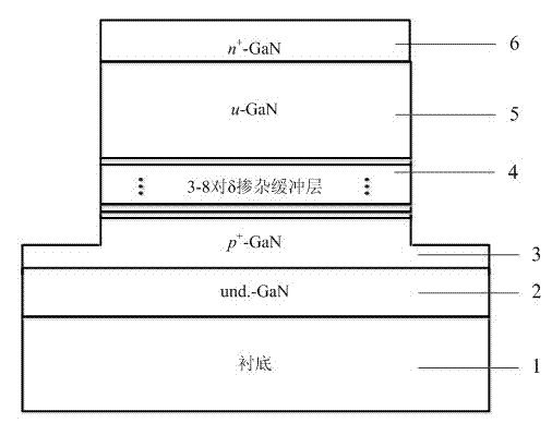
[0035] This example figure 1 A UV avalanche photodetector with a PIN inverted structure is presented, which includes: a sapphire substrate 1 and a low-temperature and high-temperature Ga N buffer layer 2, a p-type GaN layer 3, and a 3-8 pair of delta-doped buffer layer grown on it. GaN layer 4, non-doped or low-doped GaN active layer 5, n-type GaN layer 6; and n-type ohmic contact electrode 7 fabricated on n-type GaN, and p-type ohmic contact electrode 8 of p-type GaN . Taking advantage of the GaN material's characteristic of triggering holes in the avalanche process, the inverted PIN structure is adopted in the structural design. When the light signal is incident from the n-type layer, the holes are accelerated under the action of the avalanche electric field, which will maximize The gain path can greatly improve the avalanche gain of the device and suppress the dark n...


PUM


Abstract

The invention relates to an ultraviolet avalanche photodetector with a PIN inverted inversion structure and a preparation method thereof. The photodetector comprises a substrate and an epitaxial layer which grows on the substrate, wherein the epitaxial layer comprises a buffer layer, a p-type doping GaN layer, a delta doping buffer GaN layer with a plurality of cycles, an intrinsic GaN active layer with high resistance non-doping or low doping concentration and an n-type doping GaN layer from bottom to top. The preparation method of the photodetector comprises the following steps of: manufacturing a table facet and a detection window of the photodetector by utilizing photoetching and dry etching; and preparing a p-type electrode and an n-type electrode on the p-type GaN layer and the n-type GaN layer; alloying to realize ohmic contact between metal and a semiconductor. Since the n-type layer is positioned at the top layer, the incident light signal loss or the epitaxial structure defect brought about by the adoption of a back incidence mode when the p-type layer is positioned at the top side in the conventional structure is avoided, so that an electron hole triggered by light signals can obtain the maximal gain path, and therefore, the high-performance ultraviolet detector with high gain and high response is realized.

Description

technical field [0001] The invention relates to an ultraviolet detector, in particular to an ultraviolet avalanche photodetector with a PIN inverted structure and a preparation method thereof. Background technique [0002] Ultraviolet photodetectors are mainly used in military and civilian flame detection, plume detection, environmental monitoring, space optical communication, quantum communication and other fields. [0003] GaN is a third-generation semiconductor material, a new type of electronic device and optoelectronic device material, and a typical wide-bandgap semiconductor material. GaN material has the characteristics of large band gap, high electron drift saturation velocity, small dielectric constant, high temperature resistance, corrosion resistance, radiation resistance, and good thermal conductivity. It is very suitable for the production of radiation resistance, high frequency, high power and high density integration. Optoelectronic devices have become a rese...

Claims


Application Information

Patent Timeline
Patent Type & Authority Applications(China)
IPC IPC(8): H01L31/107H01L31/105H01L31/0352H01L31/18
CPCY02P70/50
Inventor 江灏李剑飞
Owner SUN YAT SEN UNIV
Why Eureka
Try Eureka