

Method for preparing tungsten-doped vanadium oxide film
A technology of tungsten oxidation and thin film, which is applied in the field of preparation of tungsten-doped vanadium oxide thin film, which can solve the problems of mutual contamination of targets and achieve the effects of stable sputtering process, avoiding mutual contamination and high temperature coefficient of resistance
- Summary
- Abstract
- Description
- Claims
- Application Information
AI Technical Summary
Problems solved by technology
Method used
Image

Examples
Embodiment 1
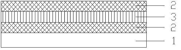
[0029] see figure 1 , figure 2 , a method for preparing a tungsten-doped vanadium oxide film, comprising the following steps:
[0030] (1) Cleaning the substrate 1;
[0031] The substrate 1 is K9 glass with a size of 22×22 mm 2 , before depositing the vanadium oxide film 2 on it, do the following cleaning: gently wipe the surface of the substrate 1 in clear water with absorbent cotton dipped in detergent, remove the dirt and dust with larger particles adsorbed in the process of cutting the substrate 1, and then Rinse several times with clean water, rinse the detergent; pour ultrapure water and put it in an ultrasonic cleaning machine for ultrasonic cleaning for 15 minutes, repeat twice to reduce the impurity ions introduced during the cleaning process with clean water; wash with ultrapure water Put the finished substrate 1 into acetone and perform ultrasonic cleaning for 15 minutes to remove insoluble organic matter, etc.; after cleaning with acetone, pour an appropriate a...
Embodiment 1
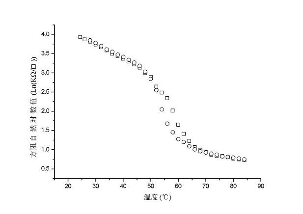
[0040] The basic process parameter of embodiment 1
[0041] background vacuum 2.0×10 -3 Pa Target surface pre-sputter cleaning time 30 minutes Substrate temperature 100 ℃ Reactive gas / working gas (O -2 / Ar) ratio 0%(W), 3.2%(VO x ) Response working pressure 1Pa sputtering current 0.3 A Sputtering film forming time 12 minutes / 20 seconds / 12 minutes Annealing temperature 350 ℃ Annealing time 15 minutes
Embodiment 2
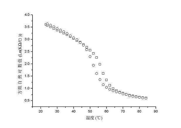
[0043] The method for preparing the tungsten-doped vanadium oxide thin film described in this embodiment is compared with that of embodiment one in that the sputtering time of the intermediate layer is 30 seconds, and the rest are the same as in embodiment one, such as image 3 As shown, the square resistance of the obtained film at 25 ℃ is 34 KΩ / □, and the temperature coefficient of resistance is -3.3 % / ℃.
PUM
| Property | Measurement | Unit |
|---|---|---|
| Temperature coefficient of resistance | aaaaa | aaaaa |
| Temperature coefficient of resistance | aaaaa | aaaaa |
| Temperature coefficient of resistance | aaaaa | aaaaa |
Abstract
Description
Claims
Application Information