A kind of organic-inorganic hybrid solar cell and preparation method thereof

A solar cell and inorganic technology, applied in the field of solar cells, can solve problems such as low photoelectric conversion efficiency, high battery manufacturing cost, and silicon quality damage, so as to reduce the probability of carrier surface recombination, enhance anti-reflection effect, reduce Effects of Purity Requirements

Inactive Publication Date: 2011-11-30
SUZHOU UNIV
View PDF6 Cites 35 Cited by
  • Summary
  • Abstract
  • Description
  • Claims
  • Application Information

AI Technical Summary

Problems solved by technology

This method needs to be heated to a very high temperature, which will also lead to an increase in the production cost of the final battery; in the process of forming p-type silicon by high temperature diffusion, the quality of silicon will be damaged due to the high heating temperature
Especially when using lower-

Method used


Image

  • A kind of organic-inorganic hybrid solar cell and preparation method thereof
  • A kind of organic-inorganic hybrid solar cell and preparation method thereof
  • A kind of organic-inorganic hybrid solar cell and preparation method thereof

Examples


Embodiment 1

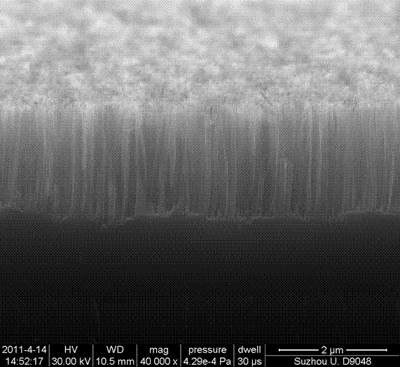
[0050] (1) Use commercial n-type silicon wafers (100) and use chlorobenzene as solvent to prepare spiro-OMeTAD solution for later use; clean the n-type silicon wafers, 3 Etched in the etching solution at room temperature for 20min, and then removed it in 30% (W / W) HNO 3 Soak in the solution for at least 1 hour to remove Ag, then rinse with deionized water to remove residual HNO 3 , to obtain a regular silicon nanowire array, the scanning electron microscope image of the silicon nanowire array is as follows image 3 shown, from image 3 It can be seen that the length of silicon nanowires is in the range of 200-2000 nm, and the distance between nanowires is 50-500 nm;

[0051] (2) In a glove box, the nanowire array was methylated by a two-step chlorination / alkylation method; the scanning electron microscope image of the silicon nanowire array is shown in Figure 4 ;

[0052] (3) Spiro-OMeTAD was then spin-coated on a silicon wafer in a glove box, and the transmission electr...

Embodiment example 2

[0058] (1) Use commercial n-type silicon wafers (100) and use chlorobenzene as solvent to prepare P3HT solution for later use; clean the n-type silicon wafers, and prepare 3 Etched in the etching solution at room temperature for 20min, and then removed it in 30% (W / W) HNO 3 Soak in the solution for at least 1 hour to remove Ag, then rinse with deionized water to remove residual HNO 3 , to obtain a regular silicon nanowire array, the electron microscope image of the silicon nanowire array is as follows image 3 shown, from image 3 It can be seen that the length of silicon nanowires is in the range of 200-2000 nm, and the distance between nanowires is 50-500 nm;

[0059] (2) In a glove box, the nanowire array was methylated by a two-step chlorination / alkylation method; the scanning electron microscope image of the silicon nanowire array is shown in Figure 4 ;

[0060] (3) Spin-coat a layer of P3HT film with a thickness of 50nm on the silicon wafer in the glove box, and th...


PUM

PropertyMeasurementUnit
Lengthaaaaaaaaaa
Thicknessaaaaaaaaaa
Thicknessaaaaaaaaaa

Abstract

The invention discloses an organic-inorganic hybridization solar battery which comprises a metal backing electrode, an n-type silicon substrate layer, a silicon nanometer wire array and a battery positive electrode and also comprises a p-type cavity transmission shell layer, wherein the p-type cavity transmission shell layer is a conjugated organic matter semiconductor thin film; the metal backing electrode is arranged on the lower surface of the n-type silicon substrate layer; the silicon nanometer wire array is arranged on the upper surface of the n-type silicon substrate layer; the surfaceof a silicon nanometer wire in the silicon nanometer wire array is covered by the layer of p-type cavity transmission shell layer; and the battery positive electrode is arranged on the p-type cavity transmission shell layer. As a three-dimensional radial p-n junction hybridization structure formed by the silicon nanometer wire array and the conjugated organic matter is adopted in the organic-inorganic hybridization solar battery, on one hand, the absorption of light is increased, the usage amount of silicon is reduced, the purify requirement on the silicon is reduced, on the other hand, the transmission range of current carriers is shortened, the problem that the current carriers are easy to combine is reduced, and the photoelectric conversion efficiency is improved.

Description

Technical field [0001] The invention relates to a solar cell, in particular to an organic-inorganic hybrid solar cell with a core-shell structure composed of organic conjugated hole transport materials and silicon nanowires. Background technique [0002] The first generation of silicon-based solar cells uses monocrystalline silicon and amorphous silicon as the main raw materials. However, on the one hand, monocrystalline silicon cells have high purity requirements for silicon wafers (more than six to nine), and the price of silicon and its purity rise exponentially. This directly leads to the high production cost of its batteries. On the other hand, the battery manufacturing process is cumbersome, which limits its large-scale commercial application. Amorphous silicon has a photofatigue effect, so the photoelectric conversion efficiency of its solar cells decreases with light. attenuation. [0003] In recent years, in order to reduce costs, simplify processes, and obtain eff...

Claims


Application Information

Patent Timeline
IPC IPC(8): H01L51/46H01L51/48
CPCY02E10/549Y02E10/50
Inventor 孙宝全张付特申小娟韩晓园雷晓飞
Owner SUZHOU UNIV
Why Eureka
Try Eureka