Cadmium-free copper indium gallium selenide thin film solar cell and preparation method of zinc sulfide buffer layer film thereof
A technology of solar cells and indium gallium selenide, which is applied in circuits, electrical components, and final product manufacturing, etc., can solve the problems of thin film non-ZnS pure phase, difficult to control thin film uniformity, and poor reproducibility of stirring rate.
- Summary
- Abstract
- Description
- Claims
- Application Information
AI Technical Summary
Problems solved by technology
Method used
Image
Examples
preparation example Construction
[0029] A method for preparing a cadmium-free copper indium gallium selenide thin film solar cell comprising the following steps:
[0030] Step 1: sequentially forming a back electrode and a CIGS light absorption layer on a substrate to form a sample.
[0031] Specifically, after the glass substrate is cleaned and placed in a vacuum chamber for glow treatment, Mo is sputtered and deposited to form a back electrode, and then transferred to another chamber for magnetron sputtering or vacuum heating to evaporate copper indium gallium metal, copper indium gallium Step-by-step deposition on the glass Mo substrate to prepare the copper indium gallium metal prefabricated layer of the CIGS thin film battery, and then transferred to the vacuum heat treatment chamber of the solid source light selenization device for solid source light selenization treatment, the copper indium gallium metal prefabricated layer layer transforms into the optically absorbing layer of the CIGS thin film cell....
Embodiment 1
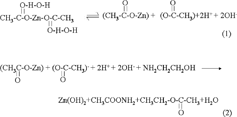
[0064] 4.39 g of Zn(CH 3 COO) 2 2H 2 O was added to 50ml of absolute ethanol, stirred until milky, and then 1.22ml of ethanolamine was added dropwise to the solution. After the solution was completely clarified, it was allowed to stand at 65°C for 10 minutes to obtain a transparent and stable zinc hydroxide sol. Dip the sample with the back electrode and CIGS light absorbing layer formed in the above-mentioned sol for 10 seconds, and slowly and evenly lift the sample out. Put the sample piece after coating film into a constant temperature oven at 120° C. to dry for 30 minutes to obtain a sample piece with ZnO thin film attached. Then in the selenization chamber H 2 Annealing in S atmosphere, the annealing temperature is 400° C., and the time is 60 minutes; a ZnS buffer layer film is obtained.
[0065] Finally, the sample with the buffer layer is transferred to the vacuum magnetron sputtering chamber to deposit the intrinsic i-ZnO high-resistance barrier layer and the low-r...
Embodiment 2
[0067] 2.195g Zn(CH 3 COO) 2 2H 2 O was added to 50ml of absolute ethanol, stirred until it became milky, and then 0.61ml of ethanolamine was added dropwise to the solution. After the solution was completely clarified, it was allowed to stand at 65°C for 10 minutes to obtain a transparent and stable zinc hydroxide sol. Dip the sample with the back electrode and CIGS light absorbing layer formed in the above-mentioned sol for 10 seconds, and slowly and evenly lift the sample out. Put the coated sample in a constant temperature oven at 100°C to dry for 30 minutes, then immerse the sample in the sol, repeat the above process several times, and obtain a sample with a suitable thickness attached to the ZnO film. Then in the selenization chamber H 2 Annealing in S atmosphere, the annealing temperature is 500° C., and the time is 10 minutes; a ZnS buffer layer film is obtained. Finally, the sample with the buffer layer is transferred to the vacuum magnetron sputtering chamber to ...
PUM
| Property | Measurement | Unit |
|---|---|---|
| Thickness | aaaaa | aaaaa |
Abstract
Description
Claims
Application Information
 - R&D
- Intellectual Property
- Life Sciences
- Materials
- Tech Scout
- Unparalleled Data Quality
- Higher Quality Content
- 60% Fewer Hallucinations
Browse by: Latest US Patents, China's latest patents, Technical Efficacy Thesaurus, Application Domain, Technology Topic, Popular Technical Reports.
© 2025 PatSnap. All rights reserved.Legal|Privacy policy|Modern Slavery Act Transparency Statement|Sitemap|About US| Contact US: help@patsnap.com


