A method of manufacturing a metal-clad laminate with improved thickness uniformity of the insulating layer
A technology of insulating layer thickness and manufacturing method, which is applied in the field of electronic materials, can solve the problems of winding edge bursting and prepreg deformation, unfavorable processing and production, and uneven force, so as to reduce the generation of substrate impurities, avoid quality control risks, strong continuity effect
- Summary
- Abstract
- Description
- Claims
- Application Information
AI Technical Summary
Problems solved by technology
Method used
Image
Examples
Embodiment 1
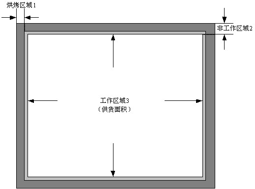
[0031] Embodiment one: see figure 1 , a method for manufacturing a metal-clad laminate that improves the thickness uniformity of an insulating layer. The process steps include: adding multifunctional epoxy resin, dicyandiamide (DICY for short), dimethylimidazole and a solvent in a certain proportion, Mix the DICY curing system glue; put the unrolled 7628 glass fiber cloth into the glue tank to soak the glue, control the glue content through the metering roller, heat and dry in the oven, and cut it directly with the shearing machine to obtain 1050mm×1265mm (longitude×weft) 7628 RC43% prepreg, the curing degree of the whole prepreg is controlled at 47±1.5%; when shearing, the prepreg is partially baked by the IR heating and baking device, and the prepreg is surrounded by 7± The curing degree of the resin within the 2mm edge area is increased to 63±2% and 72±2% respectively, and the prepreg after baking is as attached figure 1As shown, 1 is the edge area after baking, 2 is the n...
Embodiment 1-a
[0032] Example 1-a: Take a 7628 prepreg with a curing degree of 63±2% in the range of 7±2mm in the edge area, and the curing degree of the resin in the middle area is 47±1.5%, and the thickness of the laminated insulating layer is 1×7628. A thin core board of about 0.20mm is covered with 35 micron thick copper foil (hereinafter referred to as 1OZ copper foil) on both sides, and sent to a laminator to heat and pressurize to form a copper-clad laminate. The lamination and pressing process of Comparative Example 1-a is basically similar to that of Example 1-a, except that the edge area of the prepreg used is not baked, and the curing degree of the entire width is controlled at 47±1.5%.
Embodiment 1-b
[0033] Example 1-b: Take 7628 prepregs with a curing degree of 72±2% in the range of 7±2mm in the edge region, and the curing degree of the resin in the middle region is 47±1.5%, and the thickness of the laminated boards according to 5×7628 is 1.0 The copper clad laminate of about mm is covered with 18 micron thick copper foil (hereinafter referred to as 0.5OZ copper foil) on both sides, and sent to the laminator to heat and pressurize to form a copper clad laminate. The lamination and pressing process of Comparative Example 1-b is basically similar to that of Example 1-b, except that the edge area of the prepreg used in it is not baked, and the curing degree of the entire width is controlled at 47±1.5%.
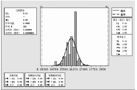
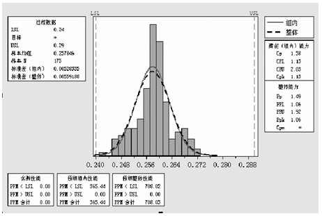
[0034] After cutting the glued edge of the plate, that is, the non-working area, a finished plate with a shipping size of 1016mm×1219.2mm (longitude×weft) is obtained. Use a 1-inch micrometer to detect about 30 plates of the two thickness specifications prepared under the ...
PUM
| Property | Measurement | Unit |
|---|---|---|
| width | aaaaa | aaaaa |
Abstract
Description
Claims
Application Information


